Conical inductor, printed circuit board and optical module
A technology of printed circuit boards and inductors, which is applied in the field of communication, and can solve problems such as pad deviation, conical inductor virtual soldering, and alignment difference.
- Summary
- Abstract
- Description
- Claims
- Application Information
AI Technical Summary
Problems solved by technology
Method used
Image

Examples
Embodiment 1
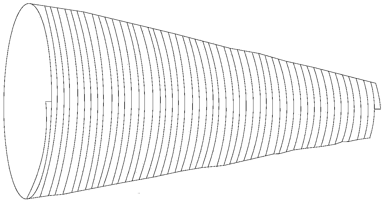
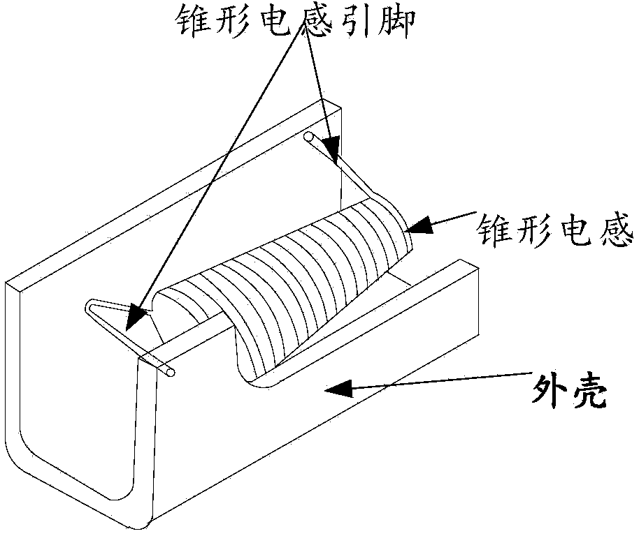
[0044] Figure 5 A schematic diagram of the composition of a tapered inductor 50 provided for an embodiment of the present invention, as shown in Figure 5 As shown, the conical inductor 50 includes: a shell 501, a conical coil 502, a first pin 503 and a second pin 504;
[0045]Wherein, the housing 501 includes a top wall 5011 and a first side wall 5012 and a second side wall 5013 connected to the top wall 501, the first side wall 5012 and the second side wall 5013 are on the side 5014 away from the top wall 5011 The positions are respectively provided with holes 5015 and 5016; the first side wall 5012 and the second side wall 5013 are in the same plane, and the first end 5014 is the end of the first side wall 5012 and the second side wall 5013 away from the top wall 5011; wherein ,It should be noted, Figure 5 The shown notch portion of the first side wall 5012 is provided for the convenience of describing the components of the tapered inductor, and does not limit the taper...
Embodiment 2
[0060] Figure 10 A structure diagram of a printed circuit board 10 provided for an embodiment of the present invention, such as Figure 10 As shown, it includes: tapered inductor 50 .
[0061] Wherein, the tapered inductor 50 is the same as the tapered inductor described in Embodiment 1, and will not be repeated here.
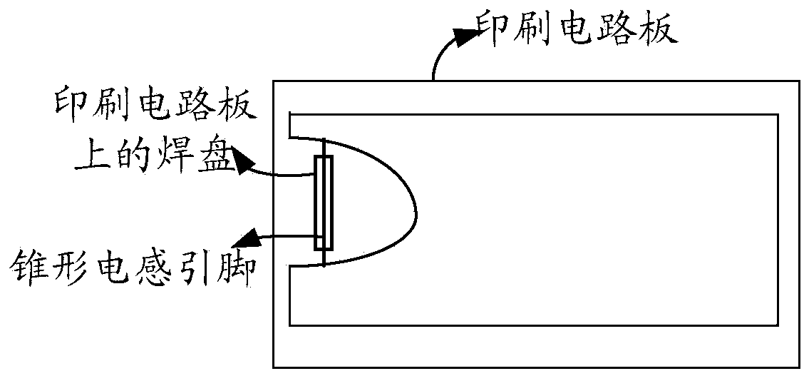
[0062] The troughs of each pin of the tapered inductor 50 are respectively fixedly connected to the printed circuit board through the solder on the pad of the printed circuit board 10 .
[0063] Preferably, the tapered inductor 50 can be soldered to the printed circuit board 10 by surface mount technology (Surface Mounted Technology, SMT for short).
[0064] As can be seen from the above, the embodiment of the present invention provides a printed circuit board 10, including a tapered inductor 50, wherein the housing includes a top wall and a first side wall and a second side wall connected to the top wall, the The first side wall and the second side wall ar...
Embodiment 3
[0066] Figure 11 A structural diagram of an optical module 11 provided for an embodiment of the present invention, such as Figure 11 As shown, the optical module 11 includes: a printed circuit board 10 .
[0067] Wherein, the printed circuit board 10 is the same as the printed circuit board in the second embodiment, which will not be repeated here.
[0068]As can be seen from the above, the embodiment of the present invention provides an optical module 11, which includes a printed circuit board 10, and the printed circuit board includes a tapered coil, wherein the housing includes a top wall and a first side wall connected to the top wall and The second side wall, the first side wall and the second side wall are respectively provided with holes on the side away from the top wall; the conical coil is located on the top wall and the first side wall, the second In the cavity formed by the side wall; one end of the first pin is connected to one end of the conical coil, and the...
PUM
 Abstract
Description
Claims
Application Information
 - Generate Ideas
- Intellectual Property
- Life Sciences
- Materials
- Tech Scout
- Unparalleled Data Quality
- Higher Quality Content
- 60% Fewer Hallucinations
Browse by: Latest US Patents, China's latest patents, Technical Efficacy Thesaurus, Application Domain, Technology Topic, Popular Technical Reports.
© 2025 PatSnap. All rights reserved.Legal|Privacy policy|Modern Slavery Act Transparency Statement|Sitemap|About US| Contact US: help@patsnap.com