Self-aligned double patterning formation method

A double pattern, self-alignment technology, applied in the direction of electrical components, semiconductor/solid-state device manufacturing, circuits, etc., can solve the problem of poor shape of the side wall of the etched pattern, and achieve the effect of not being easily deformed

Active Publication Date: 2014-06-04
SEMICON MFG INT (SHANGHAI) CORP
View PDF3 Cites 16 Cited by
  • Summary
  • Abstract
  • Description
  • Claims
  • Application Information

AI Technical Summary

Problems solved by technology

[0011] However, the inventors have found that the sidewall morphology of the etched pattern formed by etching the material layer to be etched using the above method is relatively poor.

Method used


Image

  • Self-aligned double patterning formation method
  • Self-aligned double patterning formation method
  • Self-aligned double patterning formation method

Examples


Embodiment Construction

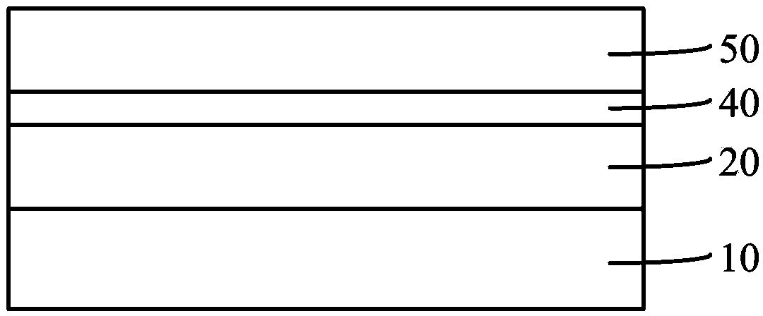
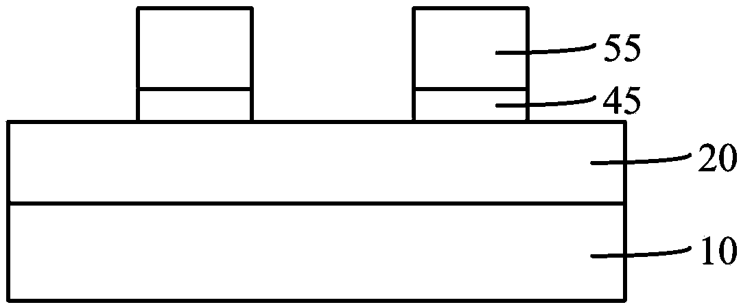
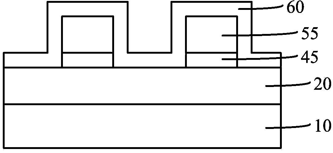
[0032] Due to the poor sidewall morphology of the etched pattern formed by etching the material layer to be etched using the above technology, the inventors have found through research that when a hard mask layer is formed on the surface of the sacrificial material layer and the sacrificial photoresist layer , the hard mask layer will exert stress on the sacrificial photoresist layer. Since the hardness of the photoresist layer is not high, the sacrificial photoresist layer is relatively soft even after exposure and baking, and the stress generated by the hard mask layer will deform the sacrificial photoresist layer, forming a trapezoidal cross section. Sacrifice the photoresist layer, so that the sidewall of the sacrificial photoresist layer is not perpendicular to the surface of the material layer to be etched, so that the sidewall subsequently formed on the sidewall surface of the sacrificial photoresist layer is not perpendicular to the material layer to be etched The surf...


PUM

PropertyMeasurementUnit
thicknessaaaaaaaaaa

Abstract

A self-aligned double patterning formation method comprises the steps of providing a material layer to be etched, forming a sacrificial photoresist layer on the material layer to be etched, forming a polymer layer on the surfaces of the top and the side walls of the sacrificial photoresist layer, forming a first mask material layer on the surface of the polymer layer, and back-etching the first mask material layer to enable the first mask material layer on the two sides of the sacrificial photoresist layer to form a first mask pattern. As the polymer layer is formed on the surfaces of the top and the side walls of the sacrificial photoresist layer, and the hardness of the polymer layer is far higher than that of the sacrificial photoresist layer, the shape of the sacrificial photoresist layer does not deform due to stress generated by the first mask material layer. Moreover, the rotation angle of the polymer layer formed by the use of a deposition process and an etching process is a right angle, which enables the sidewall morphology of the final etched pattern to be good.

Description

technical field [0001] The invention relates to semiconductor technology, in particular to a method for forming a self-aligned double pattern. Background technique [0002] In the field of semiconductor manufacturing, photoresist materials are used to transfer mask images to one or more material layers, for example, transfer mask images to metal layers, dielectric layers or semiconductor substrates. However, as the feature size of the semiconductor process continues to shrink, it becomes more and more difficult to form a mask pattern with a small feature size in the material layer by using a photolithography process. [0003] In order to improve the integration level of semiconductor devices, various double patterning processes have been proposed in the industry, among which the self-aligned double patterning (Self-Aligned Double Patterning, SADP) process is one of them. Figure 1 to Figure 6 A method for etching a semiconductor structure using a self-aligned double pattern ...

Claims


Application Information

Patent Timeline
Patent Type & Authority Applications(China)
IPC IPC(8): H01L21/033H01L21/3213
CPCH01L21/0271H01L21/033H01L21/32139
Inventor 沈满华祖延雷
Owner SEMICON MFG INT (SHANGHAI) CORP
Why Eureka
Try Eureka