High-voltage LDMOS device based on BCD process and manufacturing process
A high-voltage and process technology, applied in the field of high-voltage LDMOS devices and manufacturing processes, can solve the problems of low performance and large on-resistance of LDMOS devices, and achieve the effects of reducing on-resistance, small length of withstand voltage region, and improving withstand voltage.
- Summary
- Abstract
- Description
- Claims
- Application Information
AI Technical Summary
Problems solved by technology
Method used
Image

Examples
Embodiment Construction
[0026] The present invention will be further described below in conjunction with accompanying drawing:
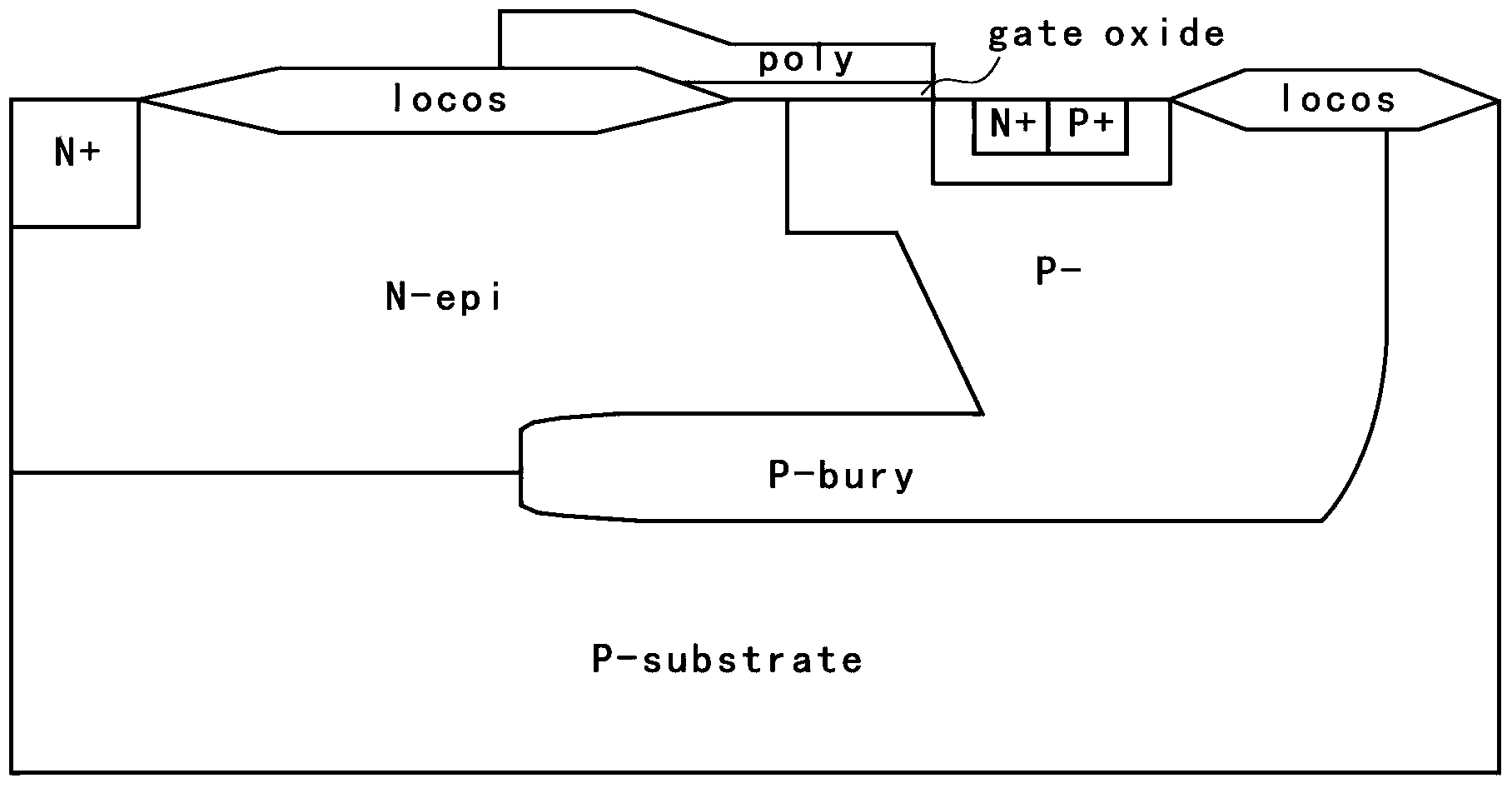
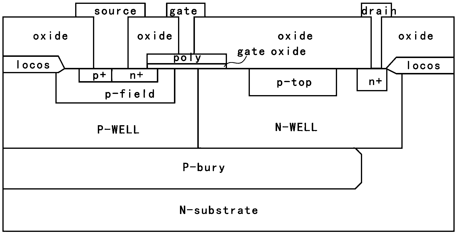
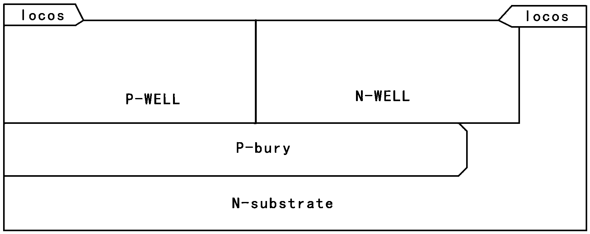
[0027] like figure 2 As shown, the high-voltage LDMOS device based on the BCD process of the present invention includes a substrate, the substrate is an N-type substrate N-substrate, and the N-type substrate N-substrate is a P-type buried layer P-bury, P The N-type thin epitaxial layer is on the buried layer P-bury, the N-well N-well is located on one side of the N-type thin epitaxial layer, and the side of the N-well N-well close to the polysilicon poly is a P-type layer covered by a field oxide layer oxide Lightly doped top layer P-top, the other side is N-type injection layer n+, N-type injection layer n+ extends upward to the drain drain, P well P-well is located on the other side of N-type thin epitaxial layer, P well P- The middle and upper part of the well is the p-type field area P-field, and the p-type field area P-field has short-circuited N-type injection layer...
PUM
| Property | Measurement | Unit |
|---|---|---|
| Thickness | aaaaa | aaaaa |
Abstract
Description
Claims
Application Information
 - R&D
- Intellectual Property
- Life Sciences
- Materials
- Tech Scout
- Unparalleled Data Quality
- Higher Quality Content
- 60% Fewer Hallucinations
Browse by: Latest US Patents, China's latest patents, Technical Efficacy Thesaurus, Application Domain, Technology Topic, Popular Technical Reports.
© 2025 PatSnap. All rights reserved.Legal|Privacy policy|Modern Slavery Act Transparency Statement|Sitemap|About US| Contact US: help@patsnap.com