Methods for manufacturing phase change memory
A phase-change memory and a technology of a manufacturing method, applied in the field of phase-change memory manufacturing, can solve problems such as poor contact performance between the phase-change layer and the bottom electrode, and achieve the effects of preventing falling off, strong process compatibility, and improving reliability
- Summary
- Abstract
- Description
- Claims
- Application Information
AI Technical Summary
Problems solved by technology
Method used
Image
Examples
Embodiment 1
[0048] Figure 2-Figure 7 Shown is a schematic structural diagram of the manufacturing method of the phase change memory provided in the first embodiment. The following combination Figure 2-Figure 7 Make a specific introduction.
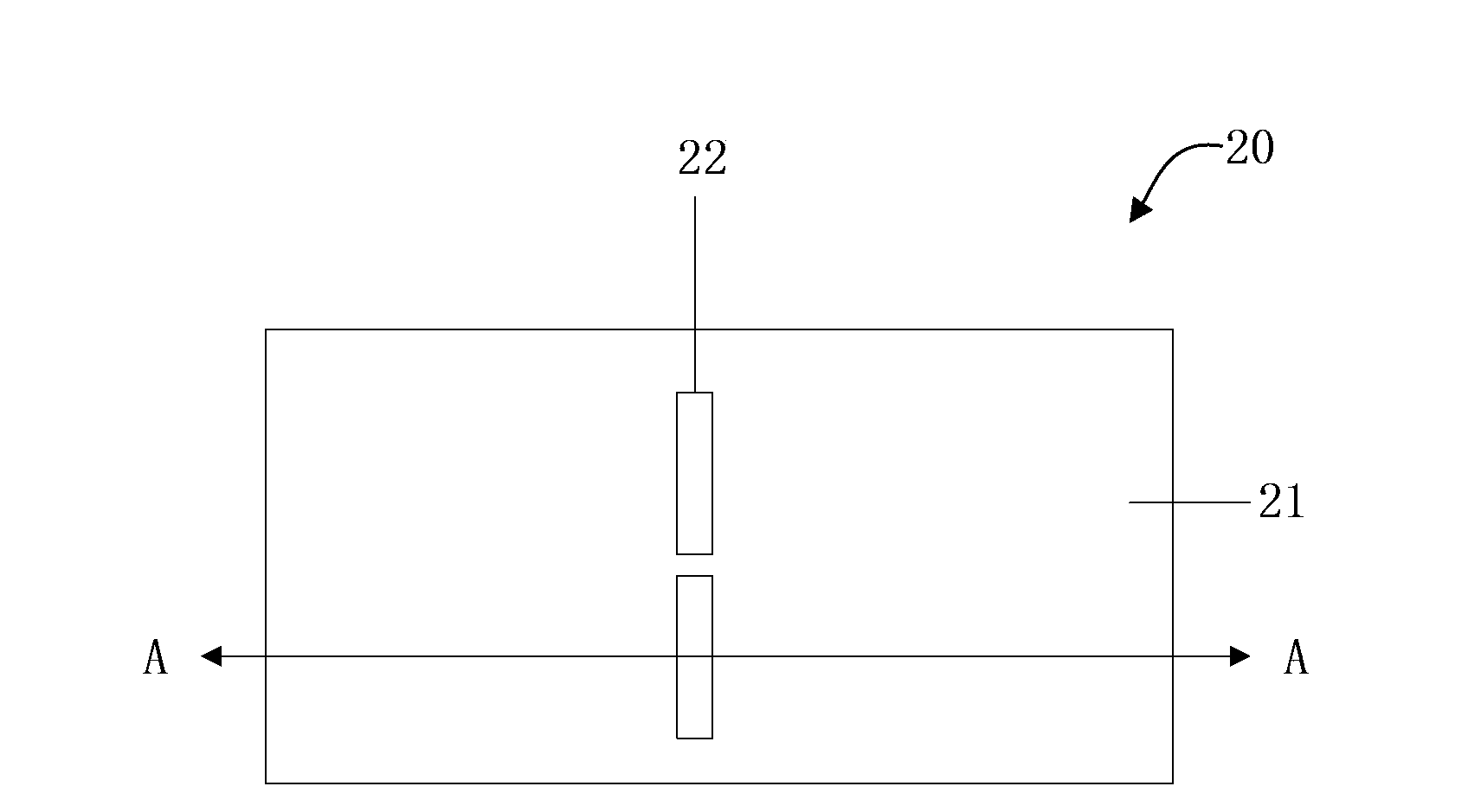
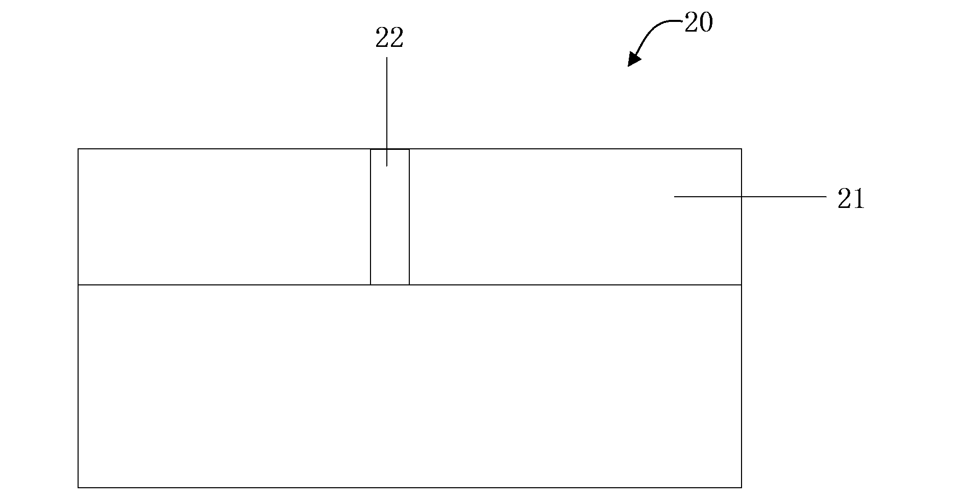
[0049] First, execute step S11: as figure 2 In the top view shown, a semiconductor substrate 20 is provided, on which at least the lower electrode 22 of the phase change memory embedded in the first dielectric layer 21 is formed. The bottom electrode 22 is also called the bottom electrode and the bottom contact structure. For the purpose of reducing the operating current of the phase change memory, it is generally in the shape of a long and narrow strip with a narrow width, for example, less than 10 nm. For the convenience of following steps, this embodiment gives figure 2 The cross-sectional structure of the A-A line in the middle is as follows image 3 shown.
[0050]The semiconductor substrate 20 can be an existing semiconductor material,...
Embodiment 2
[0071] Figure 8-Figure 10 Shown is a structural schematic diagram of another phase change memory manufacturing method provided by the invention. The following combination Figure 8-Figure 10 Make a specific introduction.
[0072] Firstly, step S21 is performed: providing a semiconductor substrate on which at least the lower electrode of the phase change memory embedded in the first dielectric layer is formed. This step is the same as the step S11 of the first embodiment, the structure of the semiconductor substrate 20, the first dielectric layer 21 thereon and the lower electrode 22 embedded in the dielectric layer 21 is still referred to figure 2 and image 3 shown.
[0073] Executing step S22: forming a second dielectric layer on the lower electrode and the first dielectric layer, and forming a trench exposing the lower electrode in the second dielectric layer by photolithography and etching. This step is the same as step S12 of Embodiment 1, and the structure of the ...
PUM
 Abstract
Description
Claims
Application Information


