Method for manufacturing thin film transistor liquid crystal displayer (TFT-LCD)

A liquid crystal display and thin film transistor technology, which is applied in the field of manufacturing ultra-thin thin film transistor liquid crystal displays, can solve problems such as bumps, increased manufacturing costs, and environmental pollution

Active Publication Date: 2014-06-18
BOE TECH GRP CO LTD +1
View PDF5 Cites 4 Cited by
  • Summary
  • Abstract
  • Description
  • Claims
  • Application Information

AI Technical Summary

Problems solved by technology

However, since the control of the cleanliness of the thinning process is far lower than that of the LCD manufacturing process, this process often causes a lot of poor appearance of the LCD, such as scratch

Method used


Image

  • Method for manufacturing thin film transistor liquid crystal displayer (TFT-LCD)
  • Method for manufacturing thin film transistor liquid crystal displayer (TFT-LCD)
  • Method for manufacturing thin film transistor liquid crystal displayer (TFT-LCD)

Examples


Embodiment Construction

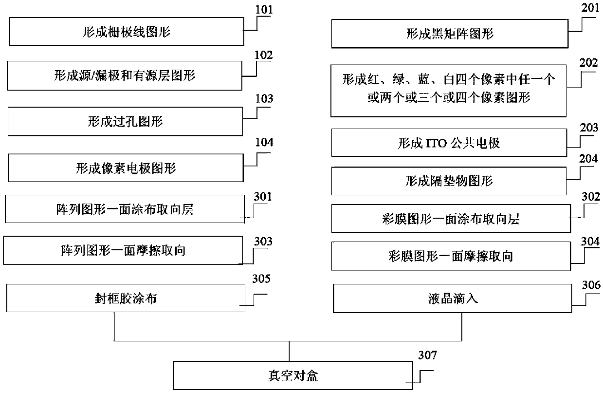
[0035] figure 1 It shows the basic process flow of manufacturing TFT-LCD in the prior art, including: array pattern formation and color filter pattern formation, and three major process flows of array substrate and color filter substrate bonding to form a liquid crystal cell.

[0036] The formation process of the array pattern can adopt the four-time mask process commonly used in this field, including:

[0037] Step 101: forming a gate line pattern;

[0038] Step 102: forming source / drain and active layer patterns;

[0039] Step 103: forming a via pattern;

[0040] Step 104: forming a pixel electrode pattern.

[0041] The forming process of color film graphics may include:

[0042] Step 201: forming a black matrix pattern;

[0043] Step 202: forming any one or two or three or four pixel graphics of red, green, blue and white pixels;

[0044] Step 203: forming an ITO common electrode;

[0045] Step 204: Form a spacer pattern.

[0046] The liquid crystal cell forming pro...


PUM

PropertyMeasurementUnit
Thicknessaaaaaaaaaa

Abstract

The invention discloses a method for manufacturing a thin film transistor liquid crystal displayer (TFT-LCD). The method for manufacturing the TFT-LCD includes: laminating a first substrate and a second substrate so as to form a mother substrate; forming an array figure on the first substrate; forming a color film figure on the second substrate; cutting the mother substrate and separating the first substrate from the second substrate; turning over the first substrate and the second substrate after being separated and forming a box. By adopting the method for manufacturing the TFT-LCD, an ultrathin thin TFT-LCD is manufactured, a subsequent thinning process is omitted, and accordingly various badness, cost increases and environmental pollution, which are caused by the subsequent process, are avoided, and furthermore green manufacturing of products is achieved.

Description

technical field [0001] The invention relates to the related technology of manufacturing thin film transistor liquid crystal display; more specifically, relates to a method of manufacturing ultrathin thin film transistor liquid crystal display. Background technique [0002] The basic principle of thin film transistor liquid crystal display (TFT-LCD) is to use thin film transistor (ThinFilm Transistor, TFT) to control and generate voltage, to control the arrangement state of liquid crystal (Liquid Crystal, LC) molecules between two glass substrates, and to use the liquid crystal material Photoelectric characteristics to generate gray scale, combined with the filter characteristics of color filter (Color Filter, CF), thus displaying a variety of rich colors. [0003] The basic structure of TFT-LCD includes an array (Array) substrate and a color filter (CF) substrate, as well as a liquid crystal layer poured between the two substrates, and a certain thickness of the box is maint...

Claims


Application Information

Patent Timeline
IPC IPC(8): G02F1/1333G02F1/136
CPCH01L27/1266G02F1/1333G02F2202/28G02F2203/68G02F1/1303H01L27/1218G02F2001/133302G02F1/133302
Inventor 莫再隆石天雷
Owner BOE TECH GRP CO LTD
Why Eureka
Try Eureka