Electric field fingerprint recognition device, state control method thereof and prosthesis identification method

A technology of fingerprint identification and electric field, which is applied in the field of fingerprint identification device and its data processing, which can solve the problems of high device cost, mutual interference of electric fields of basic units of fingerprint identification, and inability to form diversified design solutions, etc.

Active Publication Date: 2014-06-25
FOCALTECH ELECTRONICS SHENZHEN CO LTD
View PDF4 Cites 27 Cited by
  • Summary
  • Abstract
  • Description
  • Claims
  • Application Information

AI Technical Summary

Problems solved by technology

[0003] 1. Two transistors as controlled switching devices are used to realize the basic fingerprint recognition function. The structure of the basic unit of fingerprint recognition is relatively complicated, and the cost of the device is relatively high;
[0004] 2. The circuit structure is single, and it cannot form a variety of design schemes according to application requirements;
[0005] 3. There is a problem of electric field mutual interference between the fingerprint recognition basic units; there is a parasitic capacitance between the fingerprint recognition basic units, and the pa...

Method used


Image

  • Electric field fingerprint recognition device, state control method thereof and prosthesis identification method
  • Electric field fingerprint recognition device, state control method thereof and prosthesis identification method
  • Electric field fingerprint recognition device, state control method thereof and prosthesis identification method

Examples


Embodiment Construction

[0059] Further details will be given below in conjunction with the embodiments shown in the accompanying drawings.

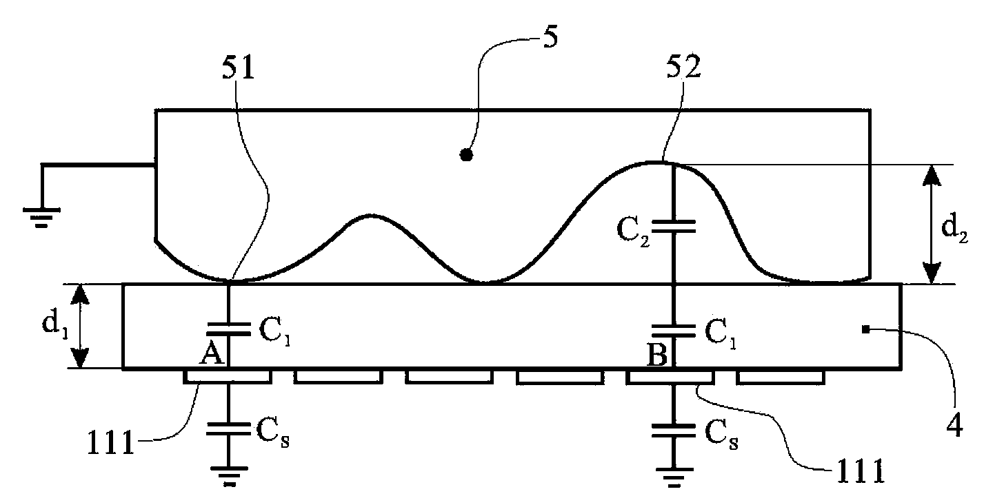
[0060] The present invention realizes the principle of fingerprint identification as figure 1 As shown, there are fingerprint raised areas 51 and fingerprint sunken areas 52 on the finger 5 . The capacitive sensing module of the fingerprint recognition device includes at least one upper plate 111 , and an insulating protective layer 4 covering each upper plate 111 . A basic capacitor Cs is formed between the upper plate 111 and the ground. When the finger 5 touches the capacitive sensing module, the capacitance between each upper plate 111 and the ground in the capacitive array of the capacitive sensing module will change.

[0061] Before touching, the capacitance at A:

[0062] After touching, the capacitance at A: ,in

[0063] The capacitance change at A before and after the touch is:

[0064] Capacitance at B before touch:

[0065] After touc...


PUM


Abstract

The invention provides an electric field fingerprint recognition device, a state control method thereof and a prosthesis identification method. The electric field fingerprint recognition device comprises a signal acquisition module and a signal processing module. When a measurement state signal processing unit is electrically connected with a signal acquisition unit, a to-be-measured state signal processing unit is at least electrically connected with at least one signal collection unit at the periphery of the measurement state signal processing unit. The charging and discharging processes of a sensing capacitor which is electrically connected to the measurement state signal processing unit and the to-be-measured state signal processing unit, and the charging and discharging quantity of electricity of a parasitic capacitor between the measurement state signal processing unit and the to-be-measured state signal processing unit is inhibited. The device and the methods have the advantages of simple structure and saving of device cost, a problem of mutual interference between signal collection units is avoided, the fingerprint recognition device can be suitable for various application requirements, a prosthesis finger fingerprint can be judged, and the safety and the reliability of the fingerprint identification device are improved.

Description

technical field [0001] The invention relates to a fingerprint identification device and a data processing method thereof, in particular to an electric field type fingerprint identification device and a data processing method thereof. Background technique [0002] Prior art electric field type fingerprint recognition device, such as Figure 13 As shown, at least one fingerprint identification basic unit is included. The fingerprint identification basic unit includes an electrode plate 71 , a first transistor 72 as a controlled switching device, a second transistor 73 as another controlled switching device, and a charge amplifier 74 . In the process of fingerprint identification, at first turn on the first transistor 72, charge the electrode plate 71, and complete the reset of the charge amplifier 74; then turn off the first transistor 72, turn on the second transistor 73, and transfer the charge on the electrode plate 71 The output terminal of the charge amplifier 74 determi...

Claims


Application Information

Patent Timeline
IPC IPC(8): G06K9/00
Inventor 莫良华胡海军
Owner FOCALTECH ELECTRONICS SHENZHEN CO LTD
Why Eureka
Try Eureka