Reaction cavity and plasma device provided with same

A reaction chamber and chamber technology, applied in the field of plasma, can solve the problems of inability to realize automatic process and automatic film transfer, and achieve the effects of simple structure, accurate control and improved process effect.

Active Publication Date: 2014-06-25
BEIJING NAURA MICROELECTRONICS EQUIP CO LTD
View PDF5 Cites 8 Cited by
  • Summary
  • Abstract
  • Description
  • Claims
  • Application Information

AI Technical Summary

Problems solved by technology

Unable to realize automatic process and automatic film transfer

Method used


Image

  • Reaction cavity and plasma device provided with same
  • Reaction cavity and plasma device provided with same
  • Reaction cavity and plasma device provided with same

Examples


Embodiment Construction

[0034] Embodiments of the present invention are described in detail below, examples of which are shown in the drawings, wherein the same or similar reference numerals designate the same or similar elements or elements having the same or similar functions throughout. The embodiments described below by referring to the figures are exemplary only for explaining the present invention and should not be construed as limiting the present invention.

[0035] In describing the present invention, it should be understood that the terms "center", "longitudinal", "transverse", "upper", "lower", "front", "rear", "left", "right", " The orientations or positional relationships indicated by "vertical", "horizontal", "top", "bottom", "inner", "outer", etc. are based on the orientation or positional relationships shown in the drawings, and are only for the convenience of describing the present invention and simplifying Describes, but does not indicate or imply that the device or element referred...


PUM


Abstract

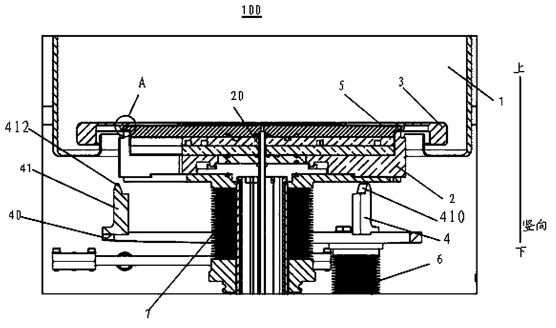
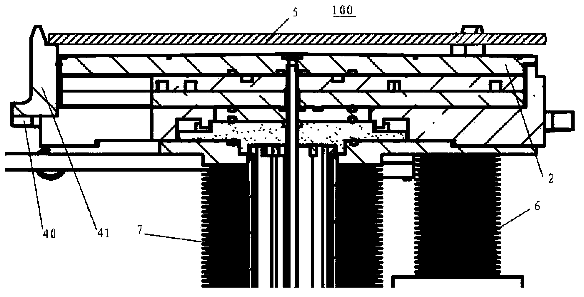
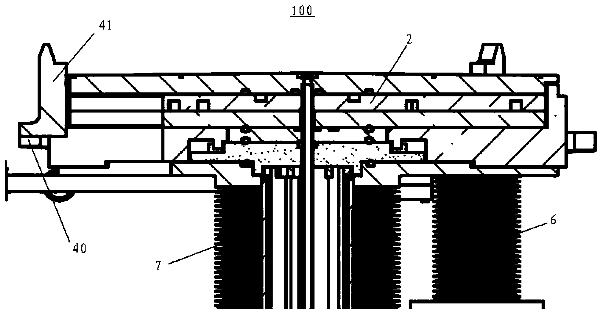
The invention discloses a reaction cavity. The reaction cavity comprises a cavity body, a pedestal, and a compaction member, wherein the pedestal is movably arranged in the cavity body between a first position and a second position below the first position along a vertical direction, the top portion of the pedestal is adapted to bearing a wafer, a gas intake and supply passage which penetrates the pedestal along the vertical direction is formed in the pedestal so as to supply process gases to the surface of the pedestal, the compaction member is provided with an inner hole, and the compaction member is arranged in such a mode that when the pedestal moves to the first position, the inner circumference of the compaction member compacts the outer edge of the wafer. According to the reaction cavity provided by the embodiments of the invention, the temperature of the wafer can be simply, rapidly and accurately controlled, the process effect of the wafer is improved, the structure of the reaction cavity is simple, and the use is convenient. The invention further discloses a plasma device provided with the reaction cavity.

Description

technical field [0001] The invention relates to the field of plasma, in particular to a reaction chamber and plasma equipment with the same. Background technique [0002] To achieve heat conduction in a vacuum environment, there must be a heat-conducting medium between the two heat-conducting objects. For example, in a vacuum reaction chamber, a silicon wafer is placed on the base. In a vacuum environment, when it needs to be heated by the base Or when cooling the silicon chip, if there is not enough thermal conductor between the two, the purpose of controlling the temperature of the silicon chip will not be achieved. [0003] A silicon chip chuck device used in the plasma process in the prior art, the silicon chip chuck device includes a lower plate and an upper plate, the upper plate is made of metal, alloy or ceramics, and has a diameter between 0.02mm and 5mm. The thickness of the lower plate is made of aluminum alloy or ceramics, the silicon chip is pressed on the lowe...

Claims


Application Information

Patent Timeline
Patent Type & Authority Applications(China)
IPC IPC(8): H01J37/32H01L21/67
Inventor 郑金果
Owner BEIJING NAURA MICROELECTRONICS EQUIP CO LTD
Why Eureka
Try Eureka