Method for forming via holes and embedded holes in multilayer circuit board

A technology of multi-layer circuit and production method, which is applied in the direction of multi-layer circuit manufacturing and the formation of electrical connection of printed components, etc., can solve the problems of high circuit production accuracy, inability to realize via holes or buried holes, and limitation of the application of laser engraving circuit technology.

Inactive Publication Date: 2014-06-25
周小平
View PDF0 Cites 4 Cited by
  • Summary
  • Abstract
  • Description
  • Claims
  • Application Information

AI Technical Summary

Problems solved by technology

At present, laser engraving circuit technology has appeared. Although the cost is high, the circuit production precision is high, the finished board is of good quality, and there is no pollution.
However,...

Method used


Image

  • Method for forming via holes and embedded holes in multilayer circuit board
  • Method for forming via holes and embedded holes in multilayer circuit board
  • Method for forming via holes and embedded holes in multilayer circuit board

Examples


Embodiment Construction

[0014] The present invention will be further described in detail below in conjunction with the accompanying drawings and specific embodiments.

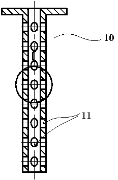
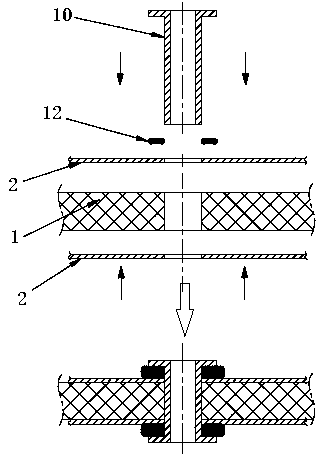
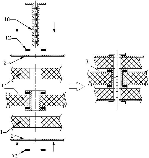
[0015] Such as figure 1 As shown, the copper pillars used in the circuit board manufacturing process in the present invention are T hollow copper pillars 10, and rows of through holes 11 are uniformly arranged at intervals of the thickness of the circuit board on the side walls of the hollow copper pillars in the vertical direction. The through holes 11 are evenly distributed in the circumferential direction of the hollow copper column, preferably in three rows of equidistant distribution in the circumferential direction of the hollow copper column, that is, a through hole is set at an interval of 120 degrees in the circumferential direction, which is enough to support welding, and the through hole will not Too small to tin. The shape of the through hole 11 can be circular or square, etc., and an ellipse is preferred for the convenie...


PUM


Abstract

The invention relates to a copper cylinder used in the manufacturing process of a circuit board. The copper cylinder is a hollow copper cylinder. Through holes are vertically formed in the side wall of the hollow copper cylinder. Based on the hollow copper cylinder, environment-friendly forming of via holes and embedded holes in a multilayer circuit board can be achieved. According to the forming method of the embedded holes, the hollow copper cylinder is arranged in the circuit board, one end or two ends of the hollow copper cylinder are welded to the circuit board, and accordingly circuits on the two sides of the circuit board can be communicated. Single-layer circuit boards and double-layer circuit boards are laminated to form the multilayer circuit board, and the through holes in the inner-layer circuit board form the embedded holes. When the embedded holes need to be connected with one certain layer of circuit board, the hollow copper cylinder is used, the hollow copper cylinder is inserted into the corresponding positions of the embedded holes from the circuit board at the uppermost layer, tin soldering is performed, and soldering tin is led in through the through holes of the hollow copper cylinder so that soldering tin and the embedded holes of the inner-layer circuit board can be welded. A brand new method for forming via holes and embedded holes in the circuit board is provided, it is hopeful that the etching technology of the circuit board can be overall improved, an electroless plating copper electroplating technology is eliminated, and energy saving and environmental protection are achieved.

Description

technical field [0001] The invention relates to the technical field of circuit boards, in particular to a method for manufacturing via holes and buried holes of a multilayer circuit board. Background technique [0002] The pollution existing in the manufacturing process of the existing multilayer circuit board is well known, and the pollution problem is a common problem in the whole industry. Each circuit board manufacturer has to spend a lot of manpower and financial resources on the prevention and control of pollution, and optimize the process as much as possible to reduce pollution. However, these process optimizations are solutions that treat the symptoms rather than the root cause. Therefore, its processing technology must be fundamentally changed. At present, laser engraving circuit technology has appeared. Although the cost is high, the circuit production precision is high, the finished board is of good quality, and there is no pollution. However, for double-sided ...

Claims


Application Information

Patent Timeline
IPC IPC(8): H05K3/40H05K3/46
Inventor 周小平
Owner 周小平
Why Eureka
Try Eureka