Scanning electron microscope equipped with back scattered electron detection function
An electron microscope and reflected electron technology, applied in circuits, discharge tubes, electrical components, etc., can solve problems such as inability to detect defects, and achieve the effect of improving detection accuracy
- Summary
- Abstract
- Description
- Claims
- Application Information
AI Technical Summary
Problems solved by technology
Method used
Image
Examples
Embodiment Construction
[0026] Before proceeding with the description of the present invention, it should be explained that in a plurality of embodiments, the same reference numerals are used for structural elements having the same structure and are representatively described in the first embodiment, and in other embodiments The structure different from that of the first embodiment will be described in the following.
[0027] Next, a scanning electron microscope having a reflection electron detection function according to a first embodiment of the present invention will be described in detail with reference to the drawings.
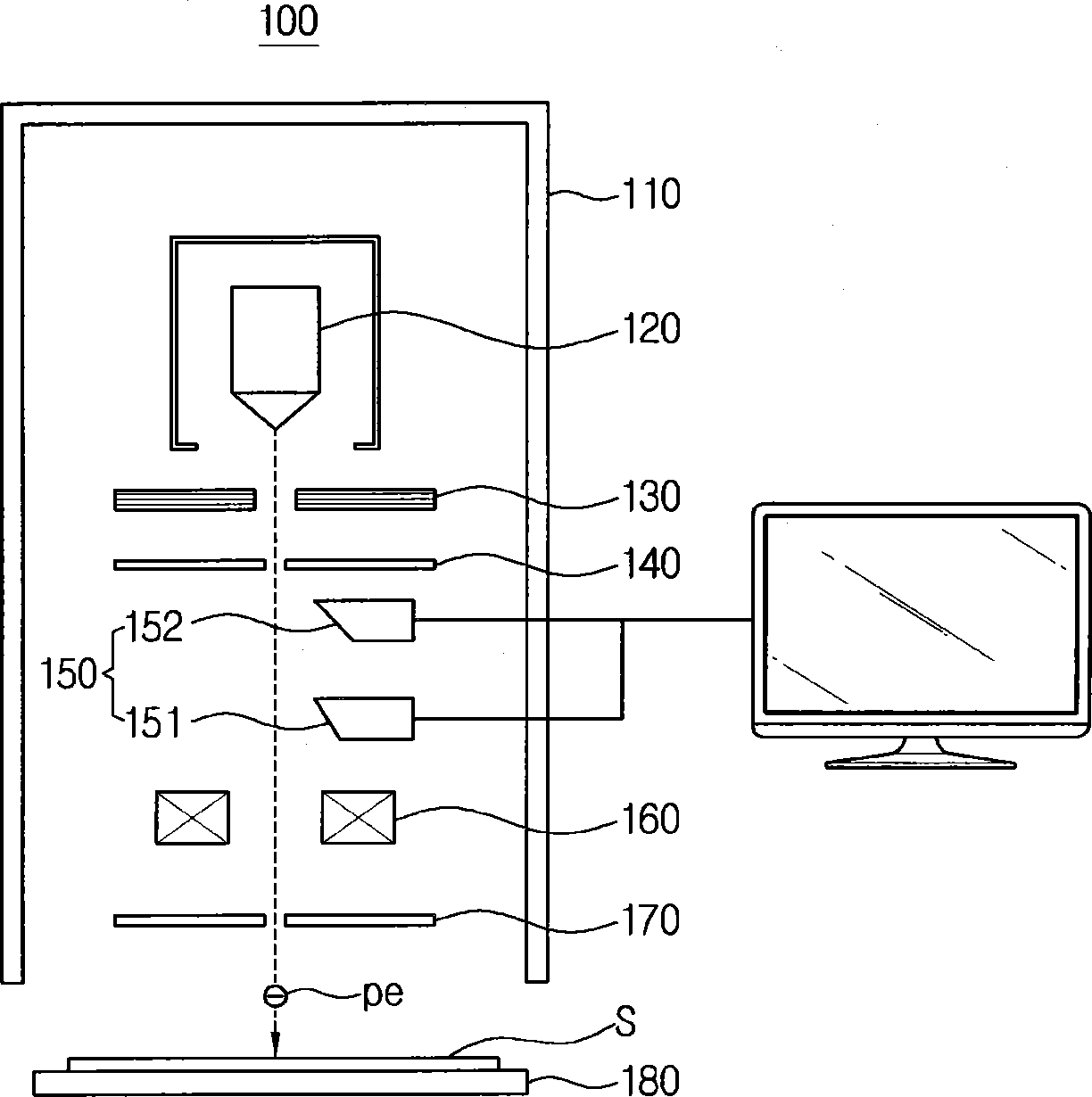
[0028] figure 2 It is a schematic cross-sectional view of a scanning electron microscope with a reflected electron detection function according to the first embodiment of the present invention.
[0029] refer to figure 2 , the scanning electron microscope 100 with the reflected electron detection function of the first embodiment of the present invention includes a lens barre...
PUM
 Abstract
Description
Claims
Application Information


