
Semiconductor device and clock data recovery system comprising semiconductor device

A semiconductor and transistor technology, applied in the fields of semiconductor devices and clock data recovery systems, can solve problems such as inability to apply a latch circuit, and achieve the effect of suppressing the decrease in gain and ensuring receiving performance

Inactive Publication Date: 2014-06-25
PANASONIC CORP
View PDF3 Cites 0 Cited by
  • Summary
  • Abstract
  • Description
  • Claims
  • Application Information

AI Technical Summary

Problems solved by technology

However, in the techniques disclosed in Patent Document 2 and Patent Document 3, the deviation of the output signal caused by the deviation of PVT, etc. is corrected by adjusting the amount of current flowing in the bias current source used to drive the circuit, so it cannot be applied to A latch circuit of the type that does not have a current source

Method used


Image

  • Semiconductor device and clock data recovery system comprising semiconductor device
  • Semiconductor device and clock data recovery system comprising semiconductor device
  • Semiconductor device and clock data recovery system comprising semiconductor device

Examples


no. 1 Embodiment approach

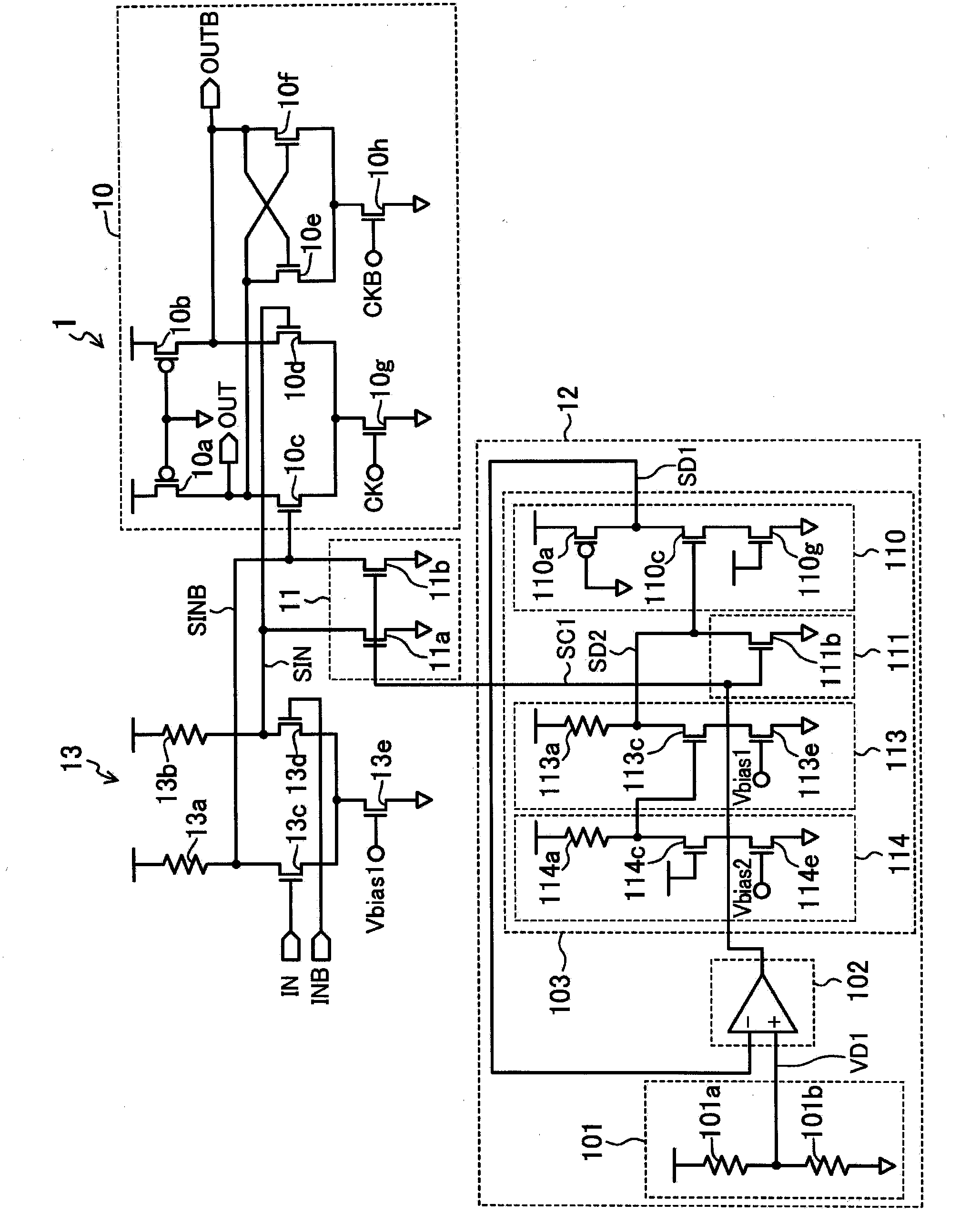
[0033] figure 1 It is a diagram showing an example of the circuit configuration of the semiconductor device according to the first embodiment of the present invention.

[0034] The latch circuit 1 includes a sampling unit 10 , a common adjustment unit 11 , and a common control unit 12 .

[0035] The sampling unit 10 includes: nMOS transistors 10c and 10d as differential pair transistors whose gates are connected to the differential input nodes SINB and SIN; and a pair of transistors whose gates are connected to the drains of the nMOS transistors 10c and 10d. The nMOS transistors 10e and 10f that constitute the holding circuit; the gate receives the clock CK as the first clock signal, and the nMOS transistor 10g that performs on-off control of the actions of the nMOS transistors 10c and 10d; the gate receives the second clock signal The clock CKB is the nMOS transistor 10h that controls the on-off operation of the nMOS transistors 10e and 10f; it is connected between the powe...

no. 2 Embodiment approach

[0075] Figure 4 It is a diagram showing an example of the circuit configuration of the semiconductor device according to the second embodiment of the present invention. Figure 4 In the semiconductor device, with figure 1 The difference is that a plurality of sampling units 10 are provided.

[0076] Figure 4 In the latch circuit 1B, the gates of the differential pair transistors 10c and 10d contained in each of the plurality of sampling units 10 are respectively connected to the differential input nodes SINB and SIN, and the differential input nodes SINB and SIN are respectively connected to the common regulator The drains of the nMOS transistors 11b and 11a of the part 11. In addition, different clocks CK0 and CK1 are supplied to the nMOS transistors 10g included in the plurality of sampling units 10, respectively. Similarly, different clocks CK0B and CK1B are supplied to the nMOS transistors 10h respectively included in the plurality of sampling units 10 . other part...

no. 3 Embodiment approach

[0086] Image 6 It is a diagram showing an example of a circuit configuration of a semiconductor device according to a third embodiment of the present invention. Image 6 In the semiconductor device, with figure 1 The difference is that it has multiple output amplifiers 13 , multiple common regulators 11 and multiple sampling units 10 .

[0087] exist Image 6 In the semiconductor device of , differential input nodes SINB, SIN and differential input nodes SINB1, SIN1 to which the output signals of the plurality of output amplifiers 13 are respectively connected are connected to gates of nMOS transistors 10c, 10d of different sampling units 10, respectively. The drains of the nMOS transistors 11b and 11a of the different common regulators 11 are connected to the differential input nodes SINB and SIN and the differential input nodes SINB1 and SIN1 respectively. In addition, different clocks CK0 and CK1 are supplied to the nMOS transistors 10 g included in the plurality of sa...


PUM


Abstract

A semiconductor device is provided with a latch circuit (1). The latch circuit (1) comprises: a sampling part (10) which latches a differential input signal which is applied from differential input nodes (SINB, SIN) to gates of differential pair transistors (10c, 10d); a common adjustment part (11) which adjusts the common potential of the differential input signal by adjusting a current value which is drawn in from the differential input nodes (SINB, SIN) on the basis of a current control signal (SC1); and a common control part (12) which controls the current control signal (SC1) such that the differential pair transistors (10c, 10d) operate in saturated regions and supplies the controlled current control signal (SC1) to the common adjustment part (11).

Description

technical field [0001] The present invention relates to a semiconductor device including a latch circuit for latching a received signal, and a clock data recovery system. Background technique [0002] Figure 8 It is a diagram showing a circuit configuration example of a latch circuit of a type that does not have a current source (for example, Patent Document 1). [0003] exist Figure 8 In the latch circuit 50, the nMOS transistor 50g is activated when the clock CK is at the High level (at this time, the clock CKB is at the Low level). Then, a current flows through the resistors 50a, 50b, and the nMOS transistors 50c, 50d, whereby the output signals OUT, OUTB change according to the input signals IN, INB. When the clock CKB is at the High level (the clock CK is at the Low level at this time), the nMOS transistor 50h is activated. Then, current flows through resistors 50a, 50b, and nMOS transistors 50e, 50f, whereby output signals OUT, OUTB are latched. [0004] Since the...

Claims


Application Information

Patent Timeline
Patent Type & Authority Applications(China)
IPC IPC(8): H03K3/3562
CPCH03K17/145H03K3/356139
Inventor 新名亮规
Owner PANASONIC CORP
Learn More