Automatic biasing band-gap reference source

A reference source and self-bias technology, which is applied in the direction of adjusting electrical variables, control/regulation systems, instruments, etc., can solve the problems of high cost and achieve the effects of fast start-up speed, high power supply rejection ratio, and power supply voltage insensitivity

Inactive Publication Date: 2014-07-02
SUZHOU VOCATIONAL UNIV
View PDF4 Cites 13 Cited by
  • Summary
  • Abstract
  • Description
  • Claims
  • Application Information

AI Technical Summary

Problems solved by technology

However, these reference source circuits use a Bipolar or BiCMOS process, and the cost is relatively high

Method used


Image

  • Automatic biasing band-gap reference source

Examples


Embodiment Construction

[0010] The present invention will be further described in detail below in conjunction with the accompanying drawings and specific embodiments.

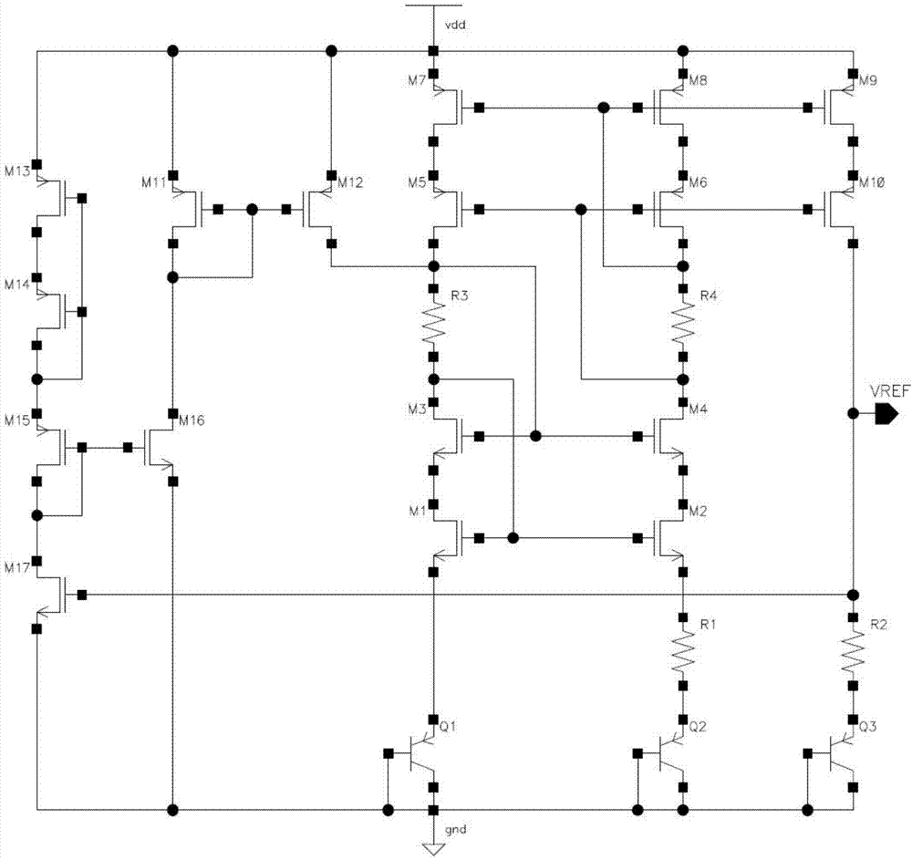
[0011] attached figure 1 The self-biased bandgap reference source of the present invention includes a reference circuit; the reference circuit includes a first cascode current mirror and a second cascode current mirror; the first cascode current mirror The current mirror includes an NMOS transistor M1, an NMOS transistor M2, an NMOS transistor M3, and an NMOS transistor M4; the second cascode current mirror includes a PMOS transistor M5, a PMOS transistor M6, a PMOS transistor M7, and a PMOS transistor M8; the A resistor R3 is connected in series in the current channel of the NMOS transistor M1, and one end of the resistor R3 is connected to the drain of the NMOS transistor M3, and is connected to the gates of the NMOS transistor M1 and the NMOS transistor M2, and provides a gate for the NMOS transistor M1 and the NMOS transistor M2. ...


PUM


Abstract

The invention discloses an automatic biasing band-gap reference source. A resistor R3 is connected into a current channel of an NMOS transistor M1 in series, one end of the resistor R3 is connected with the drain of an NMOS transistor M3 and connected with the grids of the NMOS transistor M1 and an NMOS transistor M2, grid bias voltages are provided for the NMOS transistor M1 and the NMOS transistor M2, the other end of the resistor R3 is connected with the drain of a PMOS transistor M5 and connected with the grids of the NMOS transistor M3 and an NMOS transistor M4, and grid bias voltages are provided for the NMOS transistor M3 and the NMOS transistor M4; a resistor R4 is connected into a current channel of the NMOS transistor M2 in series, one end of the resistor R4 is connected with the drain of the NMOS transistor M4 and connected with the grids of the PMOS transistor M5 and a PMOS transistor M6, grid bias voltages are provided for the PMOS transistor M5 and the PMOS transistor M6, the other end of the resistor R4 is connected with the drain of the PMOS transistor M6 and connected with the grids of a PMOS transistor M7 and a PMOS transistor M8, and grid bias voltages are provided for the PMOS transistor M7 and the PMOS transistor M8. The automatic biasing band-gap reference source is not sensitive to the power voltages, high in starting speed, low in power dissipation and temperature coefficient and high in power supply rejection ratio.

Description

technical field [0001] The invention relates to an improvement of a bandgap reference source, in particular to a self-biased bandgap reference source which is insensitive to power supply voltage, has fast starting speed, low power consumption and low temperature coefficient, and has a high power supply rejection ratio. Background technique [0002] Bandgap reference sources are widely used in various analog, digital-analog mixed-signal and power management integrated circuits. With the development of the integrated circuit industry, system-on-chip will become the mainstream of integrated circuit design in the future. A typical system-on-chip includes various digital and analog modules such as application processor module, digital signal processor module, memory unit module, analog-to-digital and digital-to-analog conversion module, voltage reference module and peripheral interface module, and the chip internal Use multiple power supplies to reduce power consumption. For the...

Claims


Application Information

Patent Timeline
Patent Type & Authority Applications(China)
IPC IPC(8): G05F1/56
Inventor 李亮
Owner SUZHOU VOCATIONAL UNIV
Why Eureka
Try Eureka