Sucking device for warped silicon wafer and sucking method thereof

A technology of adsorption device and silicon wafer, which is applied in the direction of exposure devices, instruments, electrical components, etc.

Active Publication Date: 2014-07-02
SHANGHAI MICRO ELECTRONICS EQUIP (GRP) CO LTD
View PDF3 Cites 40 Cited by
  • Summary
  • Abstract
  • Description
  • Claims
  • Application Information

AI Technical Summary

Problems solved by technology

[0007] The invention provides a warped silicon wafer adsorption device and its adsorption method to solve the problem that the silicon wafer adsorption device in the prior art cannot absorb warped silicon wafers

Method used


Image

  • Sucking device for warped silicon wafer and sucking method thereof
  • Sucking device for warped silicon wafer and sucking method thereof
  • Sucking device for warped silicon wafer and sucking method thereof

Examples


Embodiment Construction

[0031] In order to make the above objects, features and advantages of the present invention more comprehensible, specific implementations of the present invention will be described in detail below in conjunction with the accompanying drawings. It should be noted that all the drawings of the present invention are in simplified form and use inaccurate scales, and are only used to facilitate and clearly assist the purpose of illustrating the embodiments of the present invention.

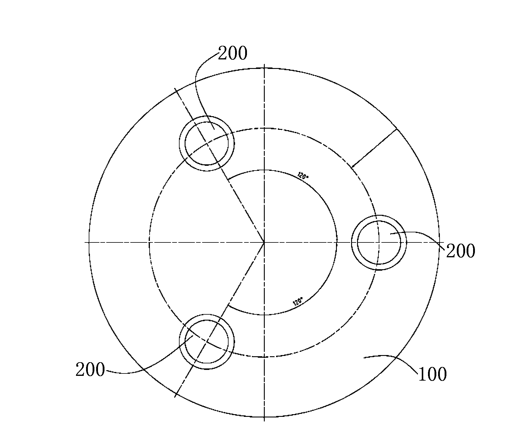
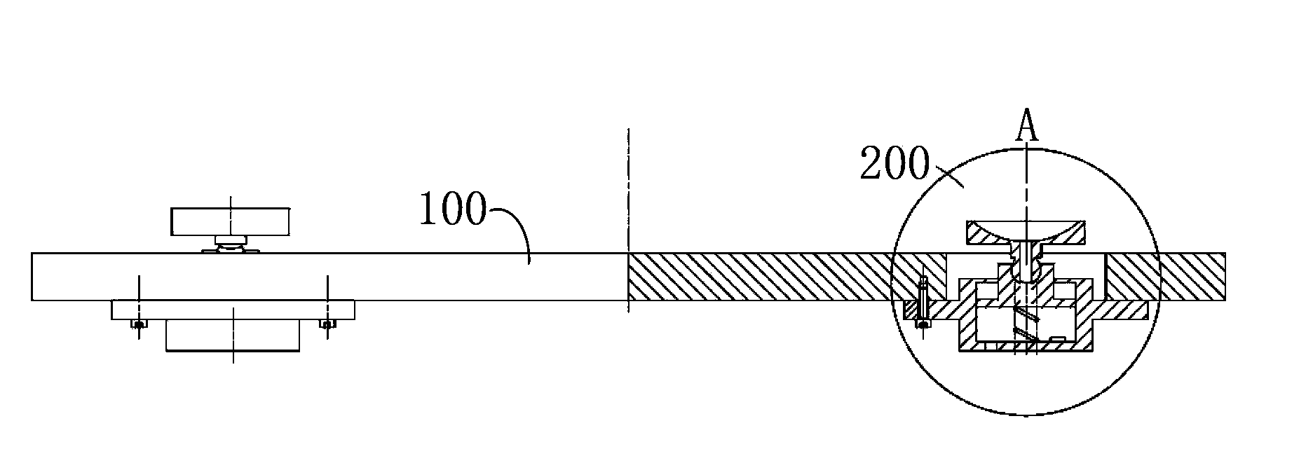
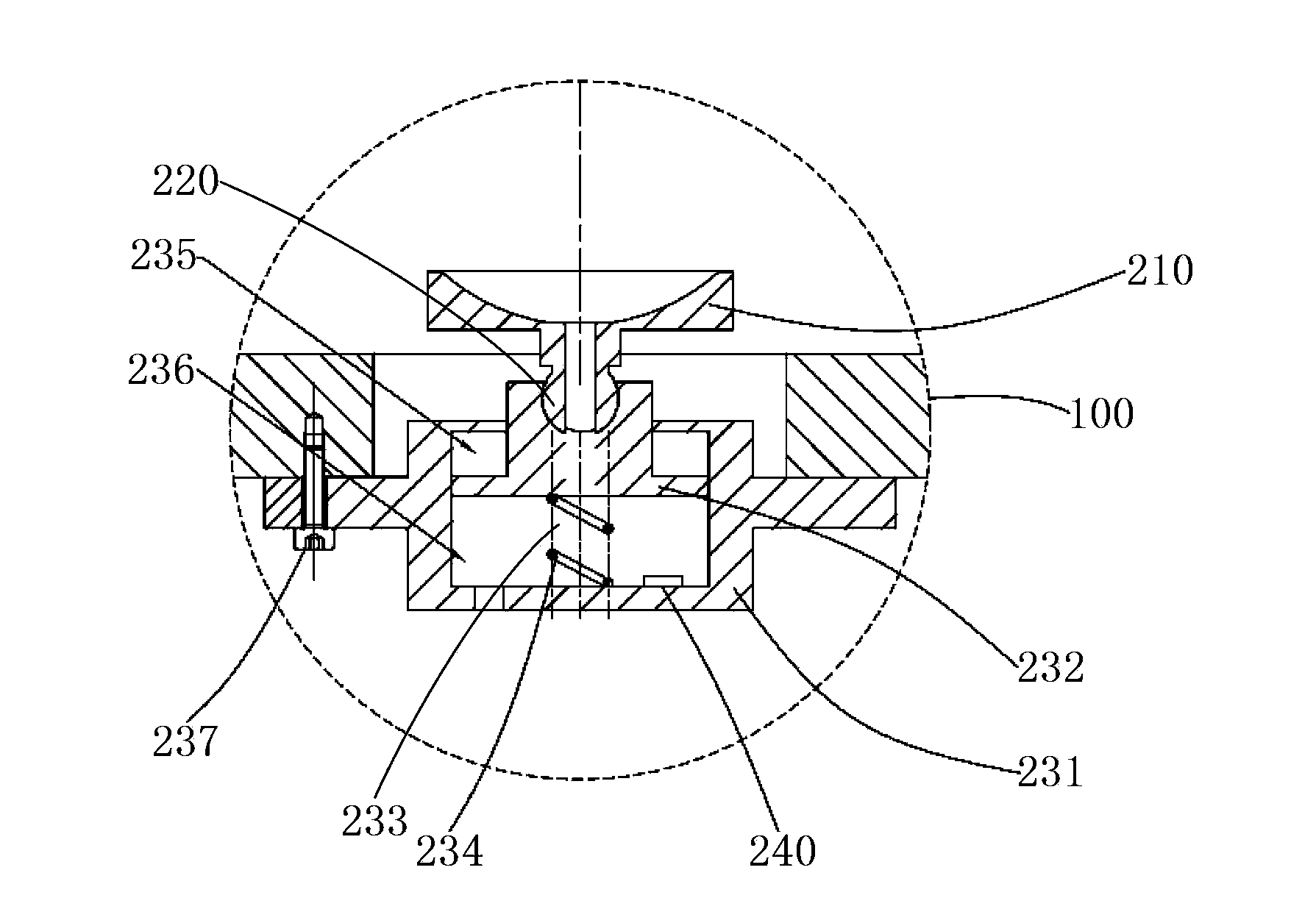
[0032] Warped silicon wafer adsorption device provided by the invention, such as figure 1 shown, and refer to Figure 2 to Figure 6 , including a suction cup 100 and at least three suction head assemblies 200 , the suction head assemblies 200 are distributed on the suction cup 100 , preferably, the suction head assemblies 200 are evenly distributed on the circumference of the suction cup 100 with equal radii. Specifically, the ratio of the distance between the center of the suction head assembly 200 an...


PUM


Abstract

A warped silicon-chip adsorption device and an adsorption method thereof. The device has a chuck (100) for vacuum adsorption of silicon-chip and at least three suction head assemblies (200). The chuck (100) has at least three openings (101), and each opening corresponds to a suction head assembly (200), wherein each suction head assembly (200) includes a cylinder (230) fixedly connected to the chuck (100), and nozzles (210) movably connected to the cylinder (230). The nozzles (210) can be all in the opening (101) or at least a portion of the nozzles (210) can be located above the surface of the chuck (100) driven by the cylinder (230). Through increasing at least three suction head assemblies (200) in the chuck (100), the warped silicon-chip (300) can be adsorbed and stretched by the suction head assembly (200) until the lower surface of the warped silicon-chip (300) is attached to the upper surface of the chuck (100), thus the adsorption of the warped silicon-chip (300) is completed.

Description

technical field [0001] The invention relates to the field of photolithography equipment, in particular to a warped silicon wafer adsorption device and an adsorption method thereof. Background technique [0002] Lithography equipment is mainly used in the manufacture of ICs (Integrated Circuit Boards) or other micro-devices. Through photolithography equipment, multi-layer masks with different mask patterns are sequentially exposed and imaged on silicon wafers coated with photoresist under precise alignment, such as semiconductor silicon wafers, LED (light emitting diode, English full name: Light Emitting Diode) LCD panel. [0003] Known lithographic apparatuses include step-and-repeat and step-and-scan. No matter what kind of lithography equipment, it is necessary to have corresponding devices as the carrier of the reticle and silicon wafer. The carrier loaded with the reticle or silicon wafer produces precise mutual movement to meet the needs of lithography. The carrier of...

Claims


Application Information

Patent Timeline
Patent Type & Authority Applications(China)
IPC IPC(8): H01L21/683H01L21/67
CPCH01L21/6838G03F7/20H01L21/67288G03F7/70783G03F7/707Y10T279/11
Inventor 王鑫鑫江旭初徐涛朱文静孙方雄孙君
Owner SHANGHAI MICRO ELECTRONICS EQUIP (GRP) CO LTD
Why Eureka
Try Eureka