Vacuum sucker for TSV silicon wafer

A vacuum suction cup and vacuum chamber technology, used in electrical components, semiconductor/solid-state device manufacturing, circuits, etc., can solve the problems of weak adsorption, difficult surface deformation, small contact area, etc., to increase the adsorption firmness and good processing performance. , Compression and rebound effect with high repeatability

Active Publication Date: 2014-07-02
SHANGHAI MICRO ELECTRONICS EQUIP (GRP) CO LTD
View PDF3 Cites 13 Cited by
  • Summary
  • Abstract
  • Description
  • Claims
  • Application Information

AI Technical Summary

Problems solved by technology

But in fact, as a bonded silicon wafer, the TSV silicon wafer has different geometric characteristics from other silicon wafers. In terms of positioning, the bottom of the TSV silicon wafer is a curved surface. See figure 1 , because the surface 101 of the traditional suction cup is made of ceramic material, the surface is not easily deformed, the contact area with the curved surface of the TSV silicon wafer 102 is small, and the adsorption is not firm

Method used


Image

  • Vacuum sucker for TSV silicon wafer
  • Vacuum sucker for TSV silicon wafer
  • Vacuum sucker for TSV silicon wafer

Examples


Embodiment 1

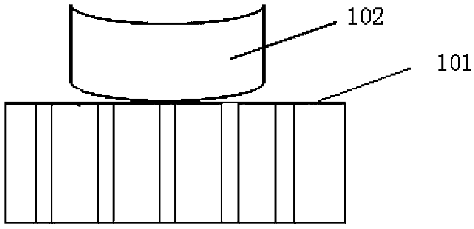
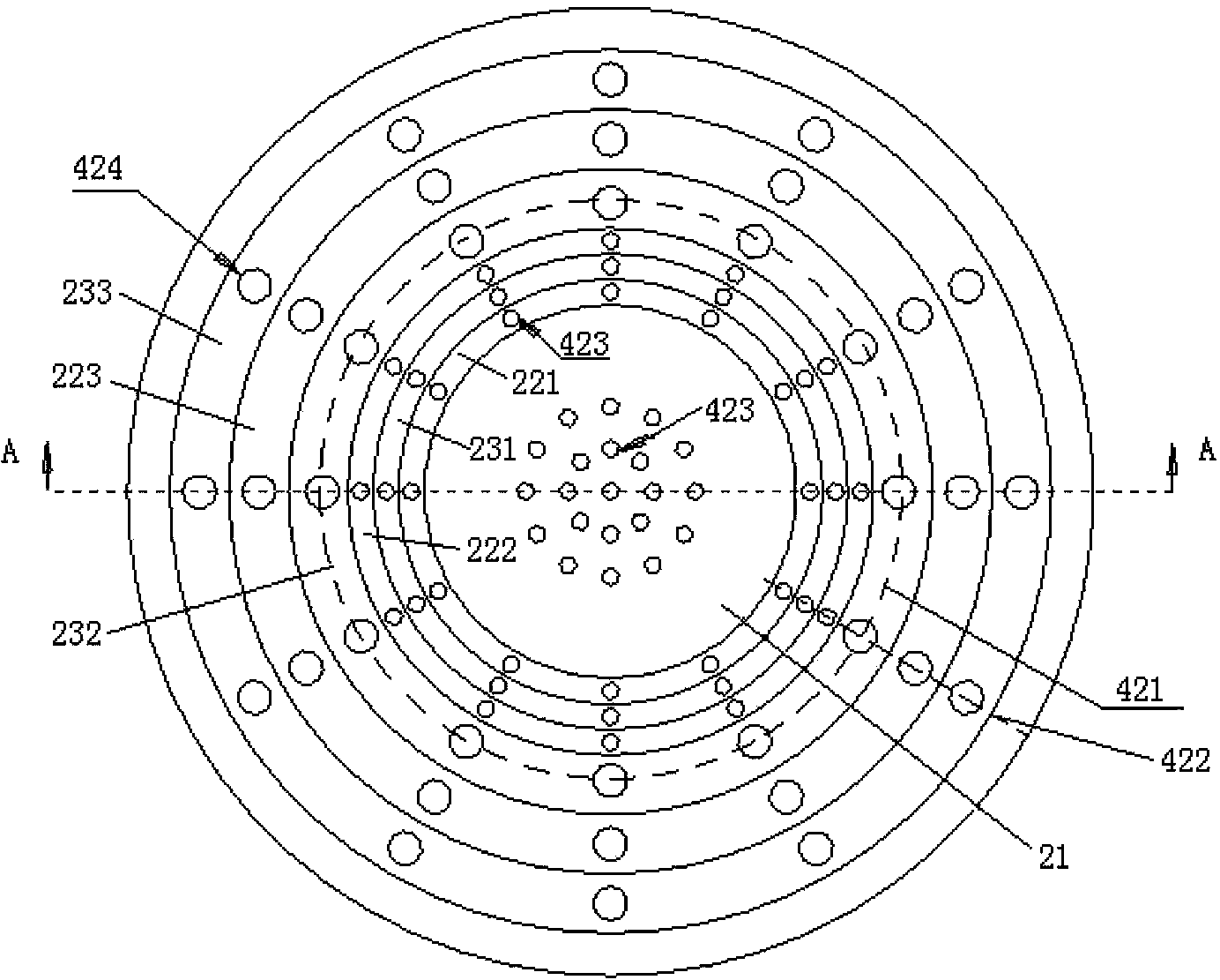
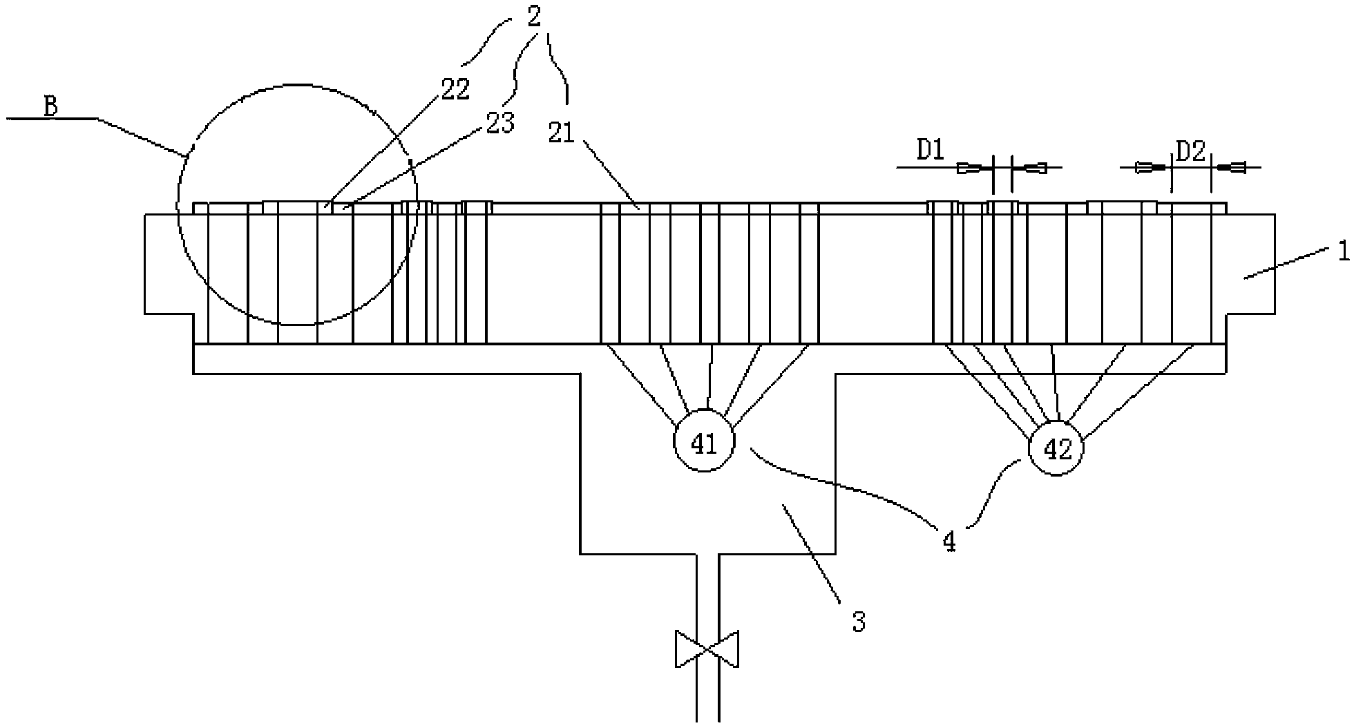
[0040] Such as figure 2 and 3 As shown, the vacuum chuck of the present invention includes a suction cup base 1, an adsorption layer 2 arranged on the upper part of the suction cup base 1, a vacuum chamber 3 arranged inside the suction cup base 1, and an adsorption layer arranged in arrays on the adsorption layer 2 and communicated with the vacuum chamber 3. Hole group 4, the adsorption layer 2 includes a central core 21 and an annular layer surrounding the core, the annular layer includes three annular elastic adsorption layers 22 and three annular rigid adsorption layers 23 arranged alternately, that is, From inside to outside are the first elastic adsorption layer 221 , the first rigid adsorption layer 231 , the second elastic adsorption layer 222 , the second rigid adsorption layer 232 , the third elastic adsorption layer 223 and the third rigid adsorption layer 233 .

[0041] The adsorption hole group 4 includes a core adsorption hole group 41 and an annular layer adsor...

Embodiment 2

[0047] Such as Figure 5 As shown, referring to Example 1, the difference is that the annular layer includes three annular elastic adsorption layers 22 interspersed with two annular rigid adsorption layers and two annular elastic adsorption layers, specifically from Inside-to-outside inner ring rigid adsorption layer 234, inner ring elastic adsorption layer 224, outer ring elastic adsorption layer 225 and outer ring elastic adsorption layer 235, the inner ring rigid adsorption layer 234 and the inner ring elastic adsorption layer 224 are provided with a small single hole 423, the adsorption holes set on the elastic adsorption layer 225 of the outer ring are porous 425, the sum of the hole areas of the porous holes 425 is greater than the small single hole 423, the large single hole 424 is set on the elastic adsorption layer 235 of the outer ring, the large single hole The pore area of ​​424 is not less than the sum of the pore areas of porous 425, and the pore diameter of a sp...


PUM


Abstract

The invention belongs to the technical field of photoetching of semiconductors, and relates to a TSV silicon wafer moving device, in particular to a vacuum sucker for a TSV silicon wafer. The vacuum sucker comprises a sucker base, an adsorption layer arranged on the upper portion of the sucker base, a vacuum chamber arranged inside the sucker base, and an adsorption hole group distributed on the adsorption layer in an array mode and communicated with the vacuum chamber, wherein the adsorption layer comprises a middle core part and an annular layer surrounding the core part, and the annular layer comprises at least one annular elastic adsorption layer and at least one annular rigid adsorption layer which are arranged in a sleeved mode. According to the sucker, the elastic adsorption layers are adopted, the adsorption area changes from inside to outside, point adsorption is changed into surface adsorption, and the firmness of TVS silicon wafer adsorption is improved; to prevent the warping of the TVS silicon wafer caused by the deformation of the elastic adsorption layers, the adsorption surface is designed in the way that the rigid adsorption layers and the elastic adsorption layers are arranged alternately in an annular mode and height difference is set, and in this way, the flatness of the TSV silicon wafer can still be kept during adsorption.

Description

technical field [0001] The invention belongs to the technical field of semiconductor lithography manufacturing, and relates to a moving device for TSV silicon wafers, in particular to a vacuum chuck for TSV silicon wafers. Background technique [0002] TSV is called Through-Silicon-Via (Through-Silicon-Via), which is a system-level integrated structure, which is formed by stacking multiple layers of silicon chips and connecting them through through holes in the normal direction of the plane. TSV silicon wafers have the advantages of the highest stacking density in three dimensions, the shortest interconnection lines between chips, the smallest size, and the ability to stack 3D chips. They are widely used in the fields of computers, communications, automotive electronics, and aerospace. [0003] In the prior art, vacuum suction cup technology is mainly used to clamp and transport silicon wafers, that is, the silicon wafers are attached to the suction cups by vacuum adsorption...

Claims


Application Information

Patent Timeline
Patent Type & Authority Applications(China)
IPC IPC(8): H01L21/683
CPCH01L21/6838
Inventor 黄明郑教增胡松立王邵玉阮冬姜晓玉
Owner SHANGHAI MICRO ELECTRONICS EQUIP (GRP) CO LTD
Why Eureka
Try Eureka