Packaging structure of OLED device and method thereof

A packaging method and packaging structure technology, which is applied in the field of OLED display, can solve the problems of glass fragility and panel cutting yield loss, and achieve the goals of reducing thermal stress, reducing overall width, improving cutting yield and sintering success rate Effect

Inactive Publication Date: 2014-07-02
EVERDISPLAY OPTRONICS (SHANGHAI) CO LTD
View PDF9 Cites 13 Cited by
  • Summary
  • Abstract
  • Description
  • Claims
  • Application Information

AI Technical Summary

Problems solved by technology

[0005] In view of the above problems, the purpose of the present invention is to reduce the thermal stress caused by the instantaneous high temperature of the glass glue in the process of laser sintering, resulting in the problem that the subsequent cutting glass is easy to break, resulting in the loss of panel cutting yield

Method used


Image

  • Packaging structure of OLED device and method thereof
  • Packaging structure of OLED device and method thereof
  • Packaging structure of OLED device and method thereof

Examples


Embodiment Construction

[0031] In order to make the object, technical solution and advantages of the present invention clearer, the present invention will be further described in detail below in conjunction with the accompanying drawings and embodiments. It should be understood that the specific embodiments described here are only used to explain the present invention, not to limit the present invention.

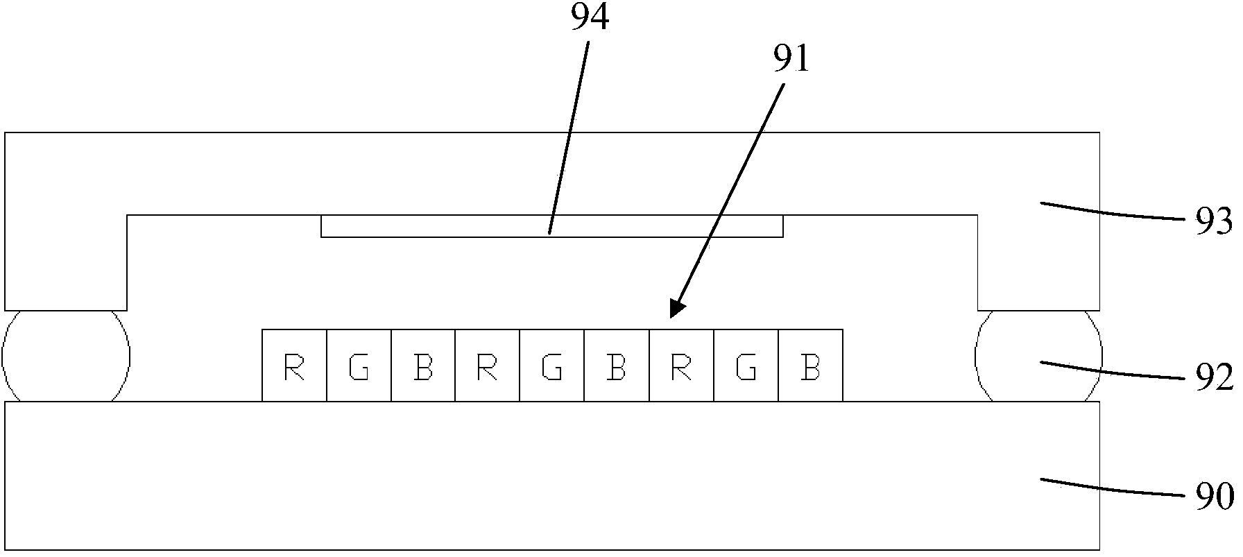
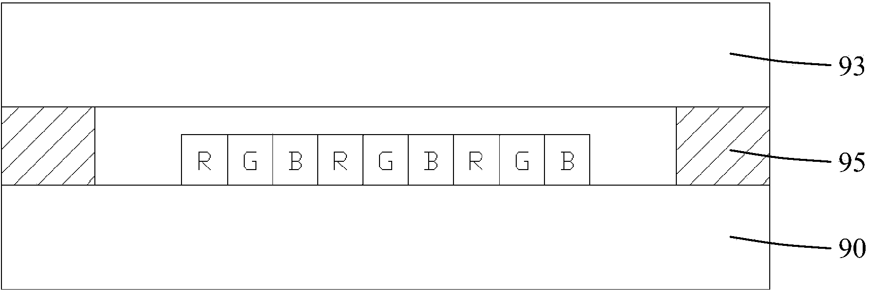
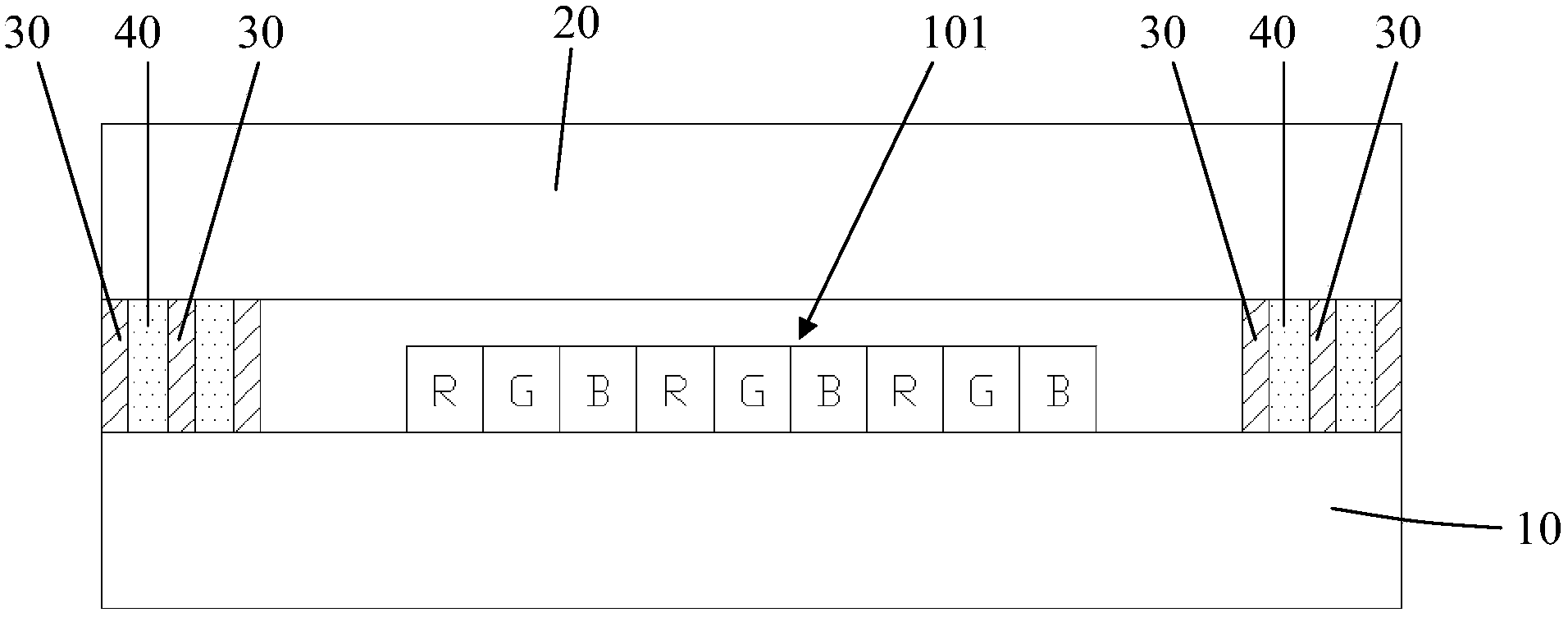
[0032] Cooperate with reference image 3 Shown, the encapsulation structure of OLED device of the present invention comprises:

[0033] A glass substrate 10, on which an OLED light-emitting unit 101 is prepared;

[0034] Glass cover plate 20, combined with Figure 4 As shown, the surface of the glass cover plate 20 near the edge is coated with a plurality of layers of glass adhesive material 30 at equal intervals along the radial direction, and a layer of buffer adhesive material is coated between two adjacent layers of the glass adhesive material 30 40 , the glass cover 30 is encapsulated on th...


PUM

PropertyMeasurementUnit
heightaaaaaaaaaa
widthaaaaaaaaaa
heightaaaaaaaaaa

Abstract

The invention discloses a packaging structure of an OLED device and a method thereof. The method comprises the following steps: (1) providing a glass substrate and preparing an OLED light unit on the glass substrate; (2) providing a glass cover plate, and coating the periphery of the surface with a plurality of layers of glass cement material in the radial direction at equal intervals, wherein the periphery of the surface is close to the edge of the glass cover plate; (3) conducting curing processing on the glass cement material; (4) attaching the glass cover plate to a glass substrate; (5) conducting sintering processing on the glass cement material, and sealing the glass cover plate to the glass substrate. Due to the fact that instant energy produced during sintering of the glass cement material is in direct proportion to the width of the glass cement material, the glass cover plate is coated with the glass cement material at equal intervals to reduce the integral width of the glass cement material, thermal stress caused by instant high temperature in the sintering process can be reduced or diffused, and the cutting yield and sintering success rate are increased.

Description

technical field [0001] The invention relates to OLED display technology, in particular to a packaging structure of an OLED device and a method thereof. Background technique [0002] An OLED device is an organic light-emitting device. Its principle is to convert electrical energy into light energy by applying a voltage to an organic material. It has the advantages of high luminous efficiency and low driving voltage. However, as the usage time increases, moisture and oxygen in the environment will easily penetrate into the device, affecting the luminous performance of the device. [0003] Traditional bottom-emission OLED packaging structure such as figure 1 As shown, the OLED device includes a glass substrate 90 on which an OLED light-emitting unit 91 is prepared. During packaging, the glass substrate 90 is bonded to the glass cover 93 through an ultraviolet light curing glue 92 (ie, UV glue). The curing glue 92 itself is poor in water resistance, so water vapor easily penet...

Claims


Application Information

Patent Timeline
Patent Type & Authority Applications(China)
IPC IPC(8): H01L51/56H01L51/52
CPCH10K50/84H10K2102/302H10K71/00
Inventor 王演隆邓学易翟宏峰赵小虎
Owner EVERDISPLAY OPTRONICS (SHANGHAI) CO LTD
Why Eureka
Try Eureka