Dislocation type electric leakage analysis method in grooved MOS device

A technology of MOS devices and analysis methods, applied in the direction of single semiconductor device testing, etc., can solve the problems of excluding dislocation defects, large limitations of TEM observation, affecting the overall analysis speed and accuracy, etc., to achieve comprehensive analysis of dislocation defects, Conducive to failure analysis and speed up the effect of process improvement

Active Publication Date: 2014-07-09
SHANGHAI HUAHONG GRACE SEMICON MFG CORP
View PDF6 Cites 4 Cited by
  • Summary
  • Abstract
  • Description
  • Claims
  • Application Information

AI Technical Summary

Problems solved by technology

[0011] 1. In the first step of EMMI analysis, the leakage point, that is, the luminous point 103 is too large, that is, the diameter of the luminous point 103 is often larger than the actual size of the dislocation defect, and it cannot quickly and completely accurately locate the dislocation defect , which affects the speed and accuracy of th

Method used


Image

  • Dislocation type electric leakage analysis method in grooved MOS device
  • Dislocation type electric leakage analysis method in grooved MOS device
  • Dislocation type electric leakage analysis method in grooved MOS device

Examples


Embodiment Construction

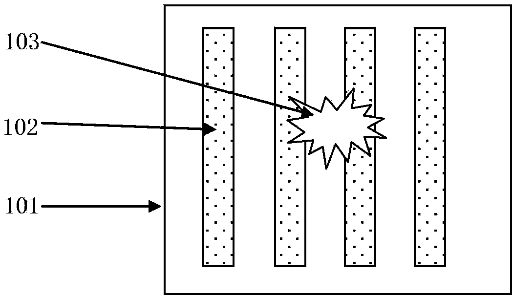
[0032] Such as Figure 4 Shown is the flow chart of the method of the embodiment of the present invention; the method for analyzing the dislocation type leakage in the trench MOS device of the embodiment of the present invention includes the following steps:

[0033] Step 1, using the EMMI analysis method to obtain defect positions in the trench MOS device chip.

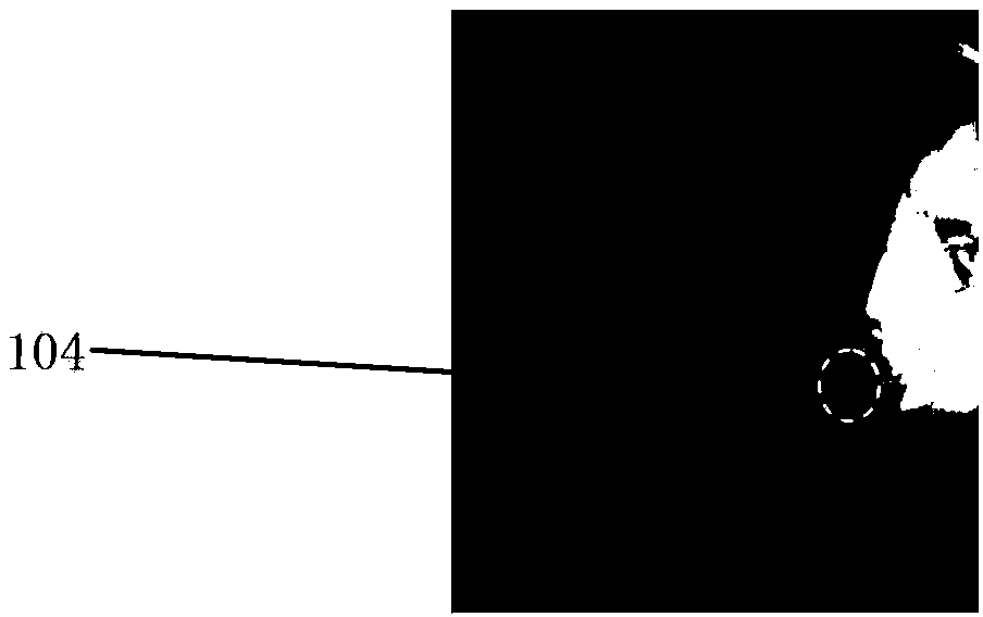
[0034] Such as Figure 5 As shown, it is a schematic diagram of EMMI positioning of failure feature points in the method of the embodiment of the present invention; a groove 2 is formed in a semiconductor substrate such as a silicon substrate 1, and a luminescent point 3 will be formed at the defect position during EMMI analysis. The defect position is revealed by using the luminous point 3 , that is, the defect position corresponds to the luminous point 3 .

[0035] The EMMI analysis conditions are controlled so that the diameter of the luminescent point 3 at the defect position is less than or equal to 1.5 micron...


PUM

PropertyMeasurementUnit
Thicknessaaaaaaaaaa

Abstract

The invention discloses a dislocation type electric leakage analysis method in a grooved MOS device. The method comprises the steps of obtaining defect positions corresponding to light emitting points through an EMMI analysis method, controlling EMMI analysis conditions to enable the diameters of the light emitting points to be smaller than or equal to 1.5 microns, preparing TEM samples at the defect positions through an FIB method, and carrying out TEM analysis on the TEM samples, wherein the centers of the TEM samples and the centers of the defect positions coincide, and the thickness of the TEM samples is larger than or equal to the diameter of the light emitting points at the defect positions. The method can be used for quickly and accurately locating, analyzing and determining electric leakage failure caused by dislocation.

Description

technical field [0001] The invention relates to a semiconductor integrated circuit manufacturing process method, in particular to a dislocation leakage analysis method in a trench MOS device. Background technique [0002] The gate array in a trench MOS device is composed of trenches, which are formed by etching a semiconductor substrate such as a silicon substrate. Dislocation defects are formed in trench MOS devices, and the dislocation defects cause leakage. When the trench MOS device has dislocation leakage, it is necessary to find out the specific position of the dislocation and analyze the dislocation. The current analysis method for dislocation type leakage in trench MOS devices includes steps: [0003] The first step is to perform EMMI (Emission Microscope, light-emitting microscope) positioning at the failure feature point. [0004] EMMI: After a non-equilibrium state is generated in a semiconductor material through a certain form of excitation, there will be a tr...

Claims


Application Information

Patent Timeline
IPC IPC(8): G01R31/26
Inventor 赖华平张君徐云
Owner SHANGHAI HUAHONG GRACE SEMICON MFG CORP
Why Eureka
Try Eureka