Multistage resistive random access memory and manufacturing method thereof

A technology of resistive variable memory and resistive variable layer, applied in static memory, digital memory information, information storage, etc., to achieve the effects of increasing stability, protecting the bottom electrode, and reducing dissipation

Inactive Publication Date: 2014-07-09
UNIV OF ELECTRONICS SCI & TECH OF CHINA
View PDF6 Cites 5 Cited by
  • Summary
  • Abstract
  • Description
  • Claims
  • Application Information

AI Technical Summary

Problems solved by technology

[0004] At present, the storage window (the ratio of high resistance to low resistance) of RRAM is generally within 10 2 -10 3 On the order of magnitude, while the storage circuit only has a storage window greater than 10 1 Therefore, the current RRAM is still a traditional two-level storage, that is, the storage state is only 0 and 1. This two-level storage mode limits the further improvement of storage density.

Method used


Image

  • Multistage resistive random access memory and manufacturing method thereof
  • Multistage resistive random access memory and manufacturing method thereof
  • Multistage resistive random access memory and manufacturing method thereof

Examples


Embodiment Construction

[0023] The present invention will be further described in detail below in conjunction with specific embodiments and accompanying drawings. It should be noted that the present invention is not limited to the embodiments.

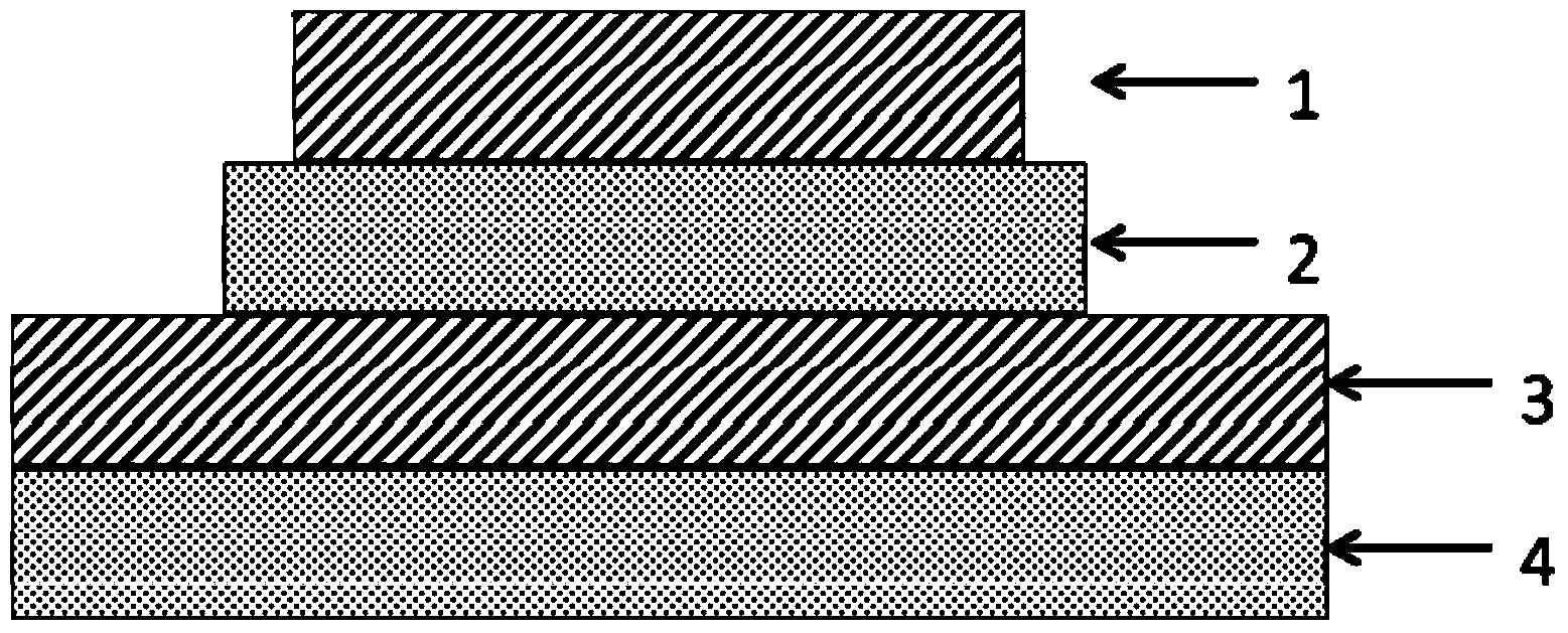
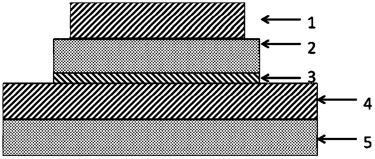
[0024] A multi-level resistive variable memory unit, comprising a substrate, a bottom electrode, a resistive variable layer, and a top electrode sequentially arranged from bottom to top; it is characterized in that an isolation layer is also arranged between the bottom electrode and the resistive variable layer. Its structure is as figure 2 shown.

[0025] In this embodiment, the multi-level resistive variable memory unit is square, and its long side and short side are both 200 microns, the material of the isolation layer is Ta, and the thickness is 2nm; the material of the resistive layer is NiO, and the thickness is 55nm; the top electrode It is a Cu film with a thickness of 150 nm and a long side and a short side of 100 micrometers. It should be noted t...


PUM


Abstract

The invention aims to provide a multistage resistive random access memory and a manufacturing method of the multistage resistive random access memory. The multistage resistive random access memory comprises a substrate, a bottom electrode, a resistive layer and a top electrode, wherein the substrate, the bottom electrode, the resistive layer and the top electrode are arranged from bottom to top in sequence. The multistage resistive random access memory is characterized in that an isolation layer is further arranged between the bottom electrode and the resistive layer. According to the multistage resistive random access memory and the manufacturing method of the multistage resistive random access memory, the nanoscale isolation layer is additionally arranged, so that the magnitude of a storage window of the resistive random access memory is increased to over 105, and the primary condition needed by multistage storage is met; electrochemical active materials are used as the top electrode, different resistance states are achieved under the condition of different voltage drives through the drifting character of the electrochemical active materials, and the purpose of multistage storage is achieved; in addition, due to the additional arrangement of the isolation layer, dissipation of oxygen ions in the movement process is reduced, the bottom electrode is effectively protected, and the stability of a device is improved. In addition, the manufacturing method of the multistage resistive random access memory is simple and easy to control.

Description

technical field [0001] The invention belongs to the technical field of electronic materials and components, and relates to information storage technology, in particular to a multi-level resistive memory unit and a preparation method thereof. Background technique [0002] At present, the storage devices on the market mainly include magnetic memory and Flash memory, such as traditional computer hard disks, U disks, and solid-state hard disks. Resistive memory mainly refers to a new type of memory that uses the reversible change of the resistance state of the resistive layer of solid components to store relevant information. Although it has not yet entered the stage of commercial application, it has broad market prospects as a recognized next-generation non-volatile memory device. [0003] The structure of the resistive memory is a multi-layer thin film structure. Its basic structure is: bottom electrode / resistive layer / top electrode, such as figure 1 shown. When the voltage...

Claims


Application Information

Patent Timeline
Patent Type & Authority Applications(China)
IPC IPC(8): H01L45/00G11C13/00B82Y10/00
Inventor 唐晓莉马国坤苏桦钟智勇张怀武荆玉兰
Owner UNIV OF ELECTRONICS SCI & TECH OF CHINA
Why Eureka
Try Eureka