Uniform light lens and LED light source module including the uniform light lens
A technology of LED light source and uniform light lens, which is applied in the direction of light source, semiconductor devices of light-emitting elements, and components of lighting devices, etc. It can solve the problems of shrinking spot radius and inability to meet the design requirements of ultra-thin direct-lit backlight, etc., and achieve fine structure , Realize the effect of uniform illumination distribution and simple mold structure
- Summary
- Abstract
- Description
- Claims
- Application Information
AI Technical Summary
Problems solved by technology
Method used
Image
Examples
Embodiment 1
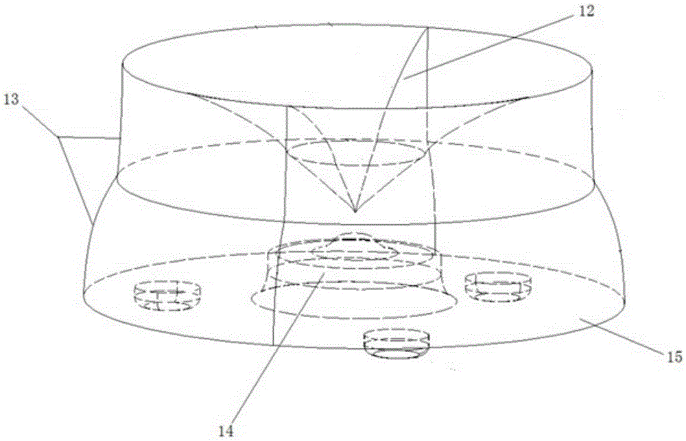
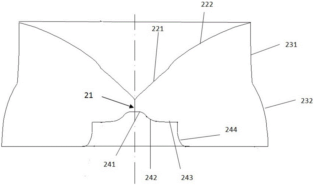
[0045] see figure 1 —3. A uniform light lens, the uniform light lens is a body of revolution, including a top exit surface 12, a side exit surface 13, an incident surface 14 and a bottom plane 15, the top exit surface 12 and the incident surface 14 are both along the A concave structure symmetrical to the axis of rotational symmetry 21 of the uniform light lens; on the section of the axis of rotational symmetry 21,
[0046] The top exit surface 12 includes an extension curve 221 and a parabola 222;
[0047] The side exit surface 13 includes a straight line segment 231 and an arc segment 232;
[0048] The incident surface 14 includes a top arc curve 241 , a first trapezoidal curve 242 , a second trapezoidal curve 243 and a lateral curve 244 connected in sequence.
[0049] In order to describe the structure of the uniform light lens more intuitively, from the cross-section, "lines" are used to describe the top exit surface, side exit surface, and incident surface; the "lines"...
Embodiment 2
[0062] see Figure 4 —5. The difference between the second embodiment and the first embodiment is that the bottom plane 15 is a frosted surface.
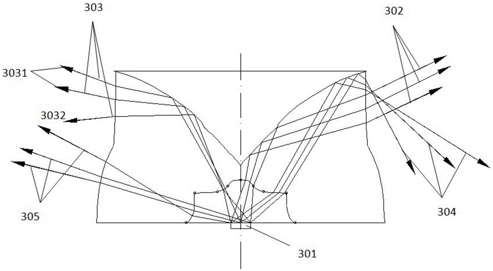
[0063] It is worth noting that in the whole design, no light directly reaches the position closest to the axis without passing through the surrounding reflective paper. This is because when the light mixing distance is extremely small, the central illuminance value should be reduced to less than 10% of the original state , bright spots may appear in any form of direct incidence. In this design, even if the original design does not directly illuminate the center, due to processing errors and light source luminous properties deviating from the design value, it is very likely that the center illuminance will be significantly higher than the surrounding area to form bright spots.
[0064] After research, it is found that the light at the position close to the edge on the lateral curve 244 has the smallest downward angle after refracti...
Embodiment 3
[0067] see Image 6 —7. The difference between the third embodiment and the first embodiment lies in that: the upper end area 502 of the straight section 231 of the side emitting surface 13 is a frosted surface, and the height of the frosted surface is≦0.5mm.
[0068] see Image 6 , due to processing errors and light source luminous properties deviating from the design value, the light 501 emitted from the LED light source 301 is incident at a position close to the edge of the second trapezoidal curve 243, reflected by the parabola 222, and then the straight line of the side exit surface 13 Segment 231 exits; since the angle at which the light 501 exits downward and reaches the reflective paper is very small, the problem of increased brightness at a position closer to the center is likely to occur after being reflected by the reflective paper. After research, it is found that this part of light 501 is concentrated on the upper end region 502 of the parabola 222 of the top ex...
PUM
 Abstract
Description
Claims
Application Information


