MEMS reflection system array, MEMS reflection system, and manufacturing method of the MEMS reflection system

A technology of reflection system and production method, which is applied in the direction of optical components, optics, instruments, etc., can solve the problems of inability to restore the original shape, easy adsorption of mirrors, etc., and achieve the effect of avoiding electrostatic adsorption

Active Publication Date: 2014-07-16
SEMICON MFG INT (SHANGHAI) CORP
View PDF5 Cites 3 Cited by
  • Summary
  • Abstract
  • Description
  • Claims
  • Application Information

AI Technical Summary

Problems solved by technology

[0008] The technical problem to be solved by the present invention is that the reflector of the MEMS reflective system is easily adsorbed on the barrier sheet and cannot be restored to its original state

Method used


Image

  • MEMS reflection system array, MEMS reflection system, and manufacturing method of the MEMS reflection system
  • MEMS reflection system array, MEMS reflection system, and manufacturing method of the MEMS reflection system
  • MEMS reflection system array, MEMS reflection system, and manufacturing method of the MEMS reflection system

Examples


Embodiment 1

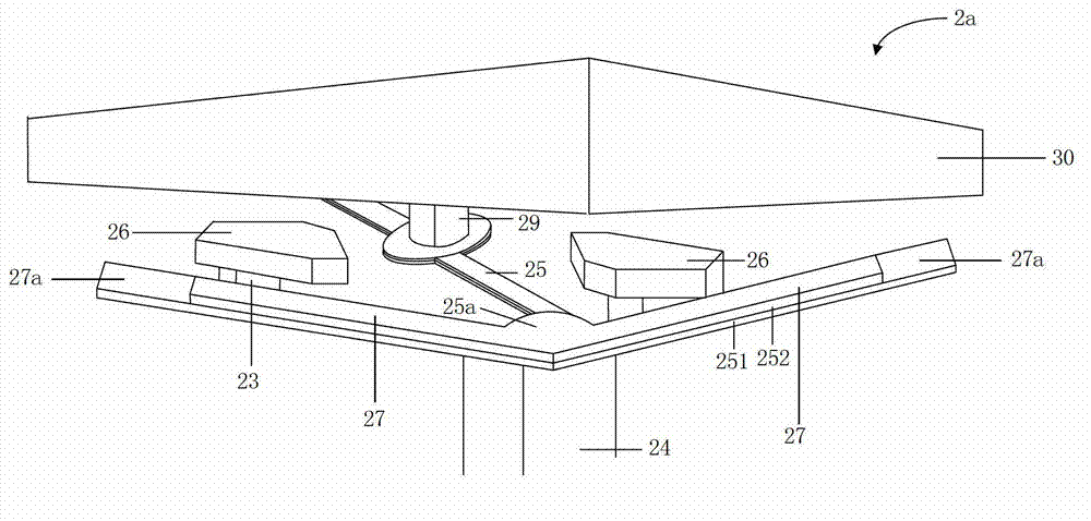
[0055] figure 2 Shown is a schematic structural diagram of the MEMS reflective system provided in this embodiment.

[0056] The MEMS reflective system includes:

[0057] A cavity 2a formed in a semiconductor substrate (not shown), and a fixed electrode 26 located in the cavity 2a;

[0058] A suspension beam 25 located in the cavity 2a, the two ends of the suspension beam 25 have support points 25a, and the support points 25a are supported by two first support columns 24 located on the semiconductor substrate;

[0059] The second support column 29 between the two support points 25a of the suspension beam, the second support column 29 is supported with a reflector 30 as a movable electrode, the reflector 30, the second support column 29, the The suspension beam 25 is electrically connected to the first support column 24;

[0060] Wherein, the two ends of the suspension beam 25 also have a blocking piece 27 for preventing the excessive deflection of the reflector 30, and the ...

Embodiment 2

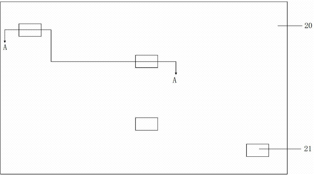
[0085] The MEMS reflective system provided in this embodiment, the manufacturing method of the reflective system and the reflective system array including multiple reflective systems are substantially the same as those in the first embodiment. The difference is that in step S2, the first sacrificial layer 22 is etched to form the first window, and when the first window is filled, the third support column 31 is also formed (refer to Figure 10 As shown), when the conductive material layer 251 and the dielectric layer 252 are etched to form the blocking sheet 27 , the blocking sheet 27 is located on the third support pillar 31 . In other words, if Figure 10 As shown, the blocking piece 27 is not only supported by the first support column 24 , but also supported by the third support column 31 . The third support pillar 31 may be electrically connected to the target electrical connection area 21 , and the conduction pattern or conductive plug is electrically connected to the tar...

Embodiment 3

[0088] The MEMS reflective system provided in this embodiment, the manufacturing method of the reflective system, and the reflective system array including a plurality of reflective systems are substantially the same as those in the first and second embodiments. The difference is: if Figure 11 As shown, in the reflective system, there is one fixed electrode 26, and the corresponding working process is: apply an electrical opposite voltage between the fixed electrode 26 and the reflector 30, and the reflector 30 is attracted by the fixed electrode 26, driving the suspension beam 25 to twist clockwise Deflection occurs, due to the existence of the blocking sheet 27, the reflector 30 will not deflect excessively and collide with the fixed electrode 26; after power failure, the reflector 30 is twisted counterclockwise under the effect of the torsional restoring force of the suspension beam 25 and returns to the equilibrium position; The same electrical voltage is applied between ...


PUM


Abstract

The invention provides an MEMS reflection system, a manufacturing method of the reflection system, and a reflection system array comprising multiple reflection systems. After frequent use of a conventional reflection system, since the whole surfaces of an over beam and a block sheet are covered by dielectric layers, during the voltage application work process of a fixation electrode and a reflector, since the reflector and the block sheet continuously bump into each other, trap charge is generated at the dielectric layer portion disposed on the block sheet, the trap charge generates a static electro adsorption phenomenon, and consequently, the reflector is absorbed to the block sheet and cannot rebound. In order to avoid such problems, the invention, the dielectric layer on the surface of a portion, which is directly contacted with the reflector, on the block sheet is at least removed, and the surface of the portion is made of a conductive material, so that the electro adsorption between the two is avoided.

Description

technical field [0001] The invention belongs to the field of semiconductor manufacturing, and in particular relates to a MEMS reflective system array, a MEMS reflective system and a manufacturing method thereof. Background technique [0002] Since the late 1980s, with the development of Micro-Electro-Mechanical-System (MEMS) technology, some semiconductor devices have been miniaturized. For example, digital micro display chips (Digital Mico Display, DMD) used in projectors, head mounted displays (Head Mounted Display), etc., which can shorten the distance between the chip and the lens, are currently being extensively studied. [0003] figure 1 Shown is the MEMS reflective system of the existing digital micro display chip, which includes a cavity 1a, a lower electrode 11 formed in the cavity 1a, a suspended beam 12 and a mirror 13 supported on the beam 12. Its working process is: apply an electrical opposite voltage between any lower electrode 11 and the reflector 13, the r...

Claims


Application Information

Patent Timeline
Patent Type & Authority Applications(China)
IPC IPC(8): G02B26/08
Inventor 叶菲周强
Owner SEMICON MFG INT (SHANGHAI) CORP
Why Eureka
Try Eureka