A tft array substrate, display panel, and display device
A technology of array substrates and substrates, which is applied in the direction of instruments, semiconductor devices, circuits, etc., can solve the problem of panel frame enlargement, achieve the effect of improving typesetting rate and reducing panel frame area
- Summary
- Abstract
- Description
- Claims
- Application Information
AI Technical Summary
Problems solved by technology
Method used
Image


Examples
Embodiment 1
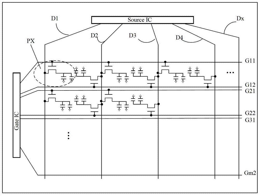
[0047] Such as Figure 2a As shown, a schematic diagram of the structure of a double-gate line array substrate disclosed in the present invention mainly includes a substrate 10, a pixel array composed of a plurality of pixels PX, TFT, a first via H, a data drive chip (Source IC), Gate drive chip (Gate IC), gate lines G11-Gm2, data lines D1-Dx and transmission lines T1-Tp.
[0048] A plurality of gate lines G11-Gm2 (where m is a positive integer) and a plurality of data lines D1-Dx (where x and n take positive integers, that is, x is the integer part of the result of (n+1) / 2), the gate lines G11-Gm2 are arranged in rows and are parallel to each other; the data lines D1-Dx are arranged in columns, and each other Parallel; the gate lines G11-Gm2 and the data lines D1-Dx are insulated to cross each other, and usually they cross vertically. The substrate can be made of transparent materials such as glass, quartz, or plastic.
[0049] In the pixel array, the pixels in the same row are ...
Embodiment 2
[0062] On the basis of the first embodiment disclosed by the present invention, the present invention discloses another dual-gate line array substrate, that is, a single driving chip IC drives the gate lines and the data lines at the same time, and the driving chip and the data lines, The gate lines are electrically connected. Therefore, the process steps can be simplified, and the cost can be reduced. At the same time, the peripheral wiring does not increase, so the layout rate will not decrease.
[0063] The specific structure is as image 3 As shown, the transmission lines T1-Tp and the data lines D1-Dx can be located on the same layer and use the same material; a driver chip IC is used to drive the gate line and the data line at the same time, that is, the data lines D1-Dx are directly electrically connected to the driver chip IC , To realize the transmission of data signals, for example, the data line D1 is directly electrically connected to the driving chip IC;
[0064] The...
Embodiment 3
[0067] On the basis of the above-mentioned first and second embodiments of the present invention, the present invention discloses another double-gate line array substrate, namely: the TFT array substrate further includes gate line leads L located in the peripheral area, and the gate line leads L The second insulating layer 14 which is between the transmission line T and electrically insulates the two passes through the second via LH of the insulating layer.
[0068] The specific structure is as Figure 4a , 4b As shown, the gate line leads L1-Lp are located in the peripheral area of the TFT array substrate, and the gate line leads L1-Lp and the gate lines G11-Gm2 are located in the same layer;
[0069] Such as Figure 4a As shown, the data lines D1-Dx are directly electrically connected to the driving chip IC, for example, the data line D1 is directly electrically connected to the driving chip IC;
[0070] Such as Figure 4b As shown, the gate line lead L and the gate line G11-Gm2 ...
PUM
 Abstract
Description
Claims
Application Information
 - R&D
- Intellectual Property
- Life Sciences
- Materials
- Tech Scout
- Unparalleled Data Quality
- Higher Quality Content
- 60% Fewer Hallucinations
Browse by: Latest US Patents, China's latest patents, Technical Efficacy Thesaurus, Application Domain, Technology Topic, Popular Technical Reports.
© 2025 PatSnap. All rights reserved.Legal|Privacy policy|Modern Slavery Act Transparency Statement|Sitemap|About US| Contact US: help@patsnap.com