
Grid drive unit, grid scanning driver and driving method of grid scanning driver

A gate drive and driver technology, applied in the direction of instruments, static indicators, etc., can solve the problems of occupying, affecting the normal operation of the circuit, and difficult to meet the high-resolution circuit design requirements

Active Publication Date: 2014-07-16
SOUTH CHINA UNIV OF TECH +1
View PDF6 Cites 16 Cited by
  • Summary
  • Abstract
  • Description
  • Claims
  • Application Information

AI Technical Summary

Problems solved by technology

Emerging transistor devices with negative voltage values, especially new oxide thin film transistors, will cause leakage current problems when used in traditional gate scanning circuits, which will affect the normal operation of the circuit
Traditional single-type (all N-type or all P-type) gate drive unit circuits still have normally-on transistors during operation, which will cause a lot of energy consumption
In addition, the charging and discharging functions of the output of most gate scan drivers are completed by two large transistors, and the driver can only be integrated on one side of the substrate, which will occupy a very large area of ​​the display substrate, resulting in uneven distribution of the substrate circuit. Symmetry is not conducive to the narrow frame effect of the display, and it is difficult to meet the high-resolution circuit design requirements

Method used


Image

  • Grid drive unit, grid scanning driver and driving method of grid scanning driver
  • Grid drive unit, grid scanning driver and driving method of grid scanning driver
  • Grid drive unit, grid scanning driver and driving method of grid scanning driver

Examples


Embodiment 1

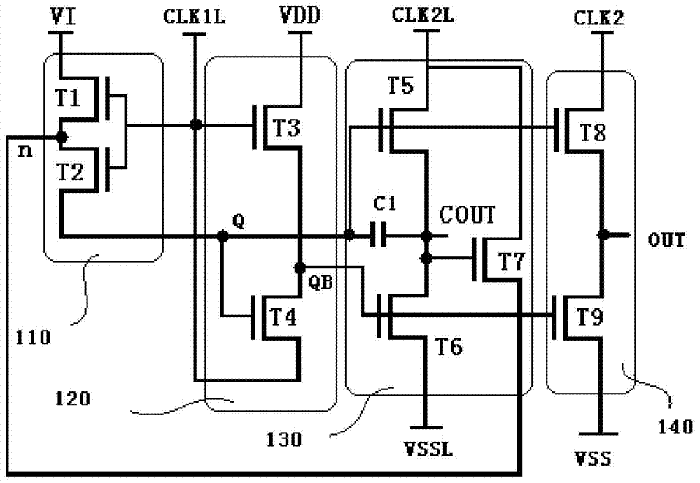
[0069] like figure 1 As shown, a gate drive unit includes an information collection module 110, an internal inverter module 120, a first signal output module 130 and a second signal output module 140;

[0070] The signal acquisition module 110 is composed of a first transistor T1 and a second transistor T2, the drain of the first transistor T1 serves as the signal acquisition port VI of the gate drive unit,

[0071] The source of the first transistor T1 is connected to the drain of the second transistor T2; the source of the second transistor T2 outputs the acquisition signal Q;

[0072] The gate of the first transistor T1 is connected to the gate of the second transistor T1 as the first clock input port CLK1L of the gate drive unit;

[0073] The internal inverter module 120 is composed of a third transistor T3 and a fourth transistor T4, the drain of the third transistor T3 is the first power input port VDD,

[0074] The gate of the third transistor T3 is connected to the f...

Embodiment 2

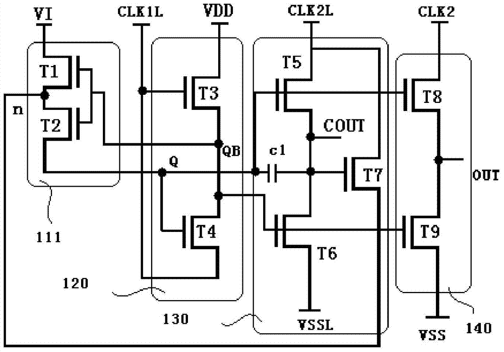
[0123] In this embodiment, if figure 2 As shown, the gate of the first transistor T1 in the signal acquisition module 111 is connected to the gate of the second transistor T2 and then connected to the output terminal QB of the internal inverter module 120 ; other features are the same as those in the first embodiment.


PUM


Abstract

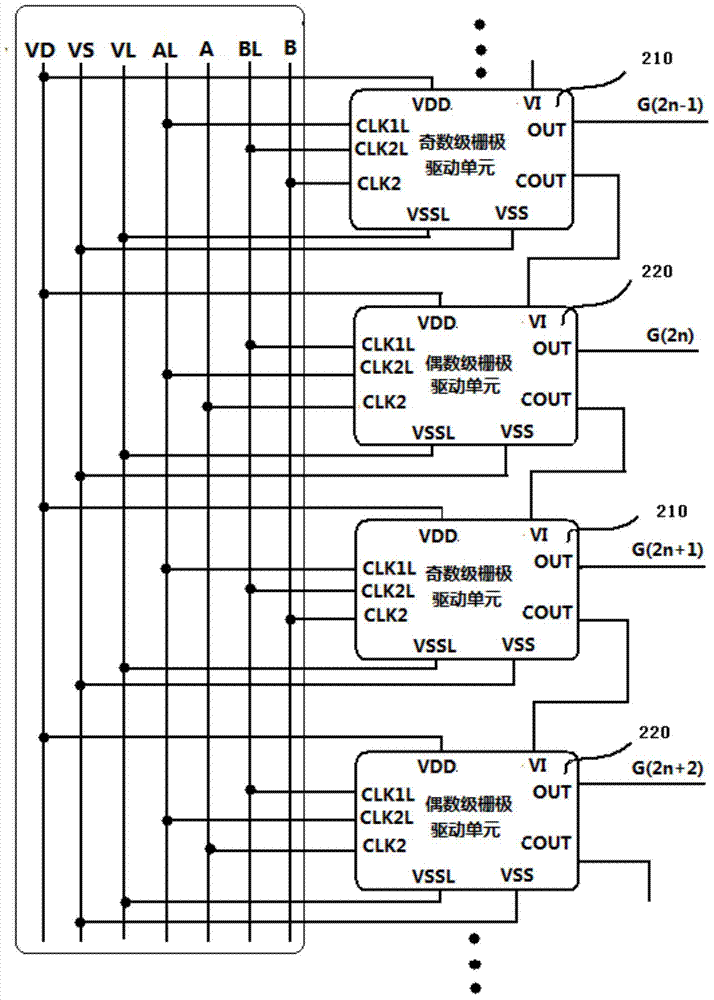
The invention discloses a grid drive unit, a grid scanning driver and a driving method of the grid scanning driver. According to the grid drive unit, clock and high level are utilized to control an internal phase inverter module to generate a low level signal, a feedback structure and a low-level and low-voltage control circuit are adopted, a direct current circuit with high level changed into low level when high level passes through a transistor is avoided, leaked current of the transistor is inhibited effectively, power consumption is reduced, and the grid drive unit is especially applicable to a transistor device with threshold voltage being a negative. The unilateral grid scanning driver constructed by the grid drive unit adopts clock signal control with 40-percent duty ratio, charging and discharging functions of a signal output end are achieved in the same transistor, and the unilateral grid scanning driver is concise in structure and low in power loss. The bilateral grid scanning driver constructed by the grid drive unit adopts clock signal control with 40-percent duty ratio and makes full use of symmetry of a screen, and narrow frame effect can be achieved in a high-definition display screen effectively.

Description

technical field [0001] The invention relates to the technical field of gate scan driving of an organic light emitting diode display, in particular to a gate drive unit, a gate scan driver and a driving method thereof. Background technique [0002] Active Matrix Organic Light Emitting Diode (AMOLED) display is a new type of display that has developed rapidly in recent years. The early AMOLED display gate row scanning driver followed the LCD driving method, and pressed a special driver chip on the glass substrate to drive the pixel circuit through the COG process. In recent years, due to the development of FPD technology, integrated gate drive technology has attracted great interest in the industry. Using the integrated gate scanning driver to drive the gate of the display pixel circuit can reduce the use of the driver chip, reduce the production cost, and can also reduce the loss of signal transmission and improve the display quality. [0003] The thin film transistors used...

Claims


Application Information

Patent Timeline
Patent Type & Authority Applications(China)
IPC IPC(8): G09G3/32G09G3/3225
Inventor 吴为敬李冠明张立荣夏兴衡周雷徐苗王磊彭俊彪
Owner SOUTH CHINA UNIV OF TECH
Learn More