PMOS transistor and manufacturing method thereof

A transistor and conductor technology, applied in the field of PMOS transistors and their preparation, can solve the problems of increasing static power consumption, device driving capability and speed reduction, large power consumption, etc., to avoid stress release, high carrier mobility, The effect of improving the working current

Active Publication Date: 2014-07-16
SEMICON MFG INT (SHANGHAI) CORP
View PDF3 Cites 6 Cited by
  • Summary
  • Abstract
  • Description
  • Claims
  • Application Information

AI Technical Summary

Problems solved by technology

In the process of shrinking device size proportionally, higher integration and operating frequency mean greater power consumption. Reducing the power supply voltage VDD is a general choice to reduce circuit power consumption, but the reduction of VDD will cause the drive of the device Decreased power and speed
Reducing the threshold voltage and thinning the thickness of the gate dielectric can improve the current driving capability of the device, but at the same time it will lead to an increase in the subthreshold leakage current and the gate leakage current, thereby increasing the static power consumption. This is the current "power consumption" faced by ICs. -speed" dilemma

Method used


Image

  • PMOS transistor and manufacturing method thereof
  • PMOS transistor and manufacturing method thereof
  • PMOS transistor and manufacturing method thereof

Examples


preparation example Construction

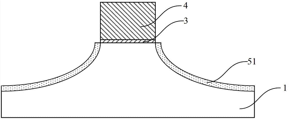
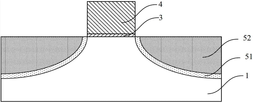
[0049] In view of this, the present invention provides a kind of preparation method of PMOS transistor, comprises the following steps at least: Provide a semiconductor substrate, form the source region, drain region and channel region on the top of the semiconductor substrate of prefabricated PMOS transistor active region, and the source region and the drain region exert compressive stress on the channel region; wherein, the specific steps of preparing the source region and the drain region are: 1) on the top of the substrate Pre-preparing the positions of the source region and the drain region respectively to form trenches; 2) In the trenches, first epitaxially grow the first stress adjustment layer, and then epitaxially grow the second stress adjustment layer, wherein the The lattice constants of the substrate, the first stress adjustment layer, and the second stress adjustment layer increase sequentially; 3) Repeat step 2) n times, where n is an integer and greater than or e...

Embodiment 1

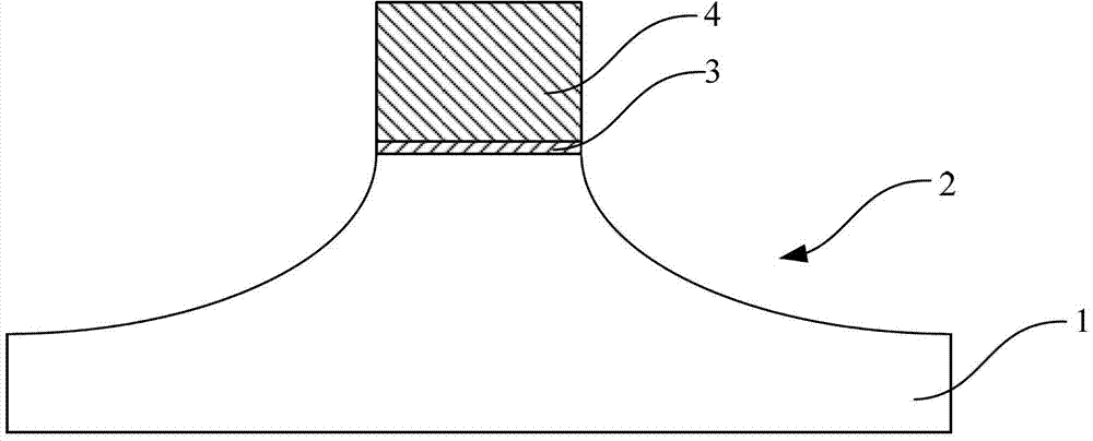
[0052] Such as Figure 1 to Figure 4 As shown, the present invention provides a preparation method of a PMOS transistor, the preparation method at least includes the following steps: providing a semiconductor substrate 1, forming a source region, a drain region and an The active region of the channel region, and the source region and the drain region exert compressive stress on the channel region; wherein, the specific steps of preparing the source region and the drain region are:

[0053] First perform step 1), such as figure 1 As shown, grooves 2 are respectively formed on the top of the substrate 1 where the source region and the drain region are pre-prepared, wherein the shape of the cross section of the groove 2 is not limited, and may be circular or sigma. etc., in this embodiment, the cross-sectional shape of the trench 2 is as figure 1 shown. It should be pointed out that, figure 1 Among them, between the trenches 2 and formed on the surface of the substrate 1 ar...

Embodiment 2

[0068] The technical solution of embodiment 2 is basically the same as that of embodiment 1, the only difference is that step 2) is repeated n times in step 3) of the preparation method in embodiment 1, and the value of n is 0; the PMOS transistor in embodiment 1 In the source region and the drain region, the value of m of the first stress adjustment layer and the second stress adjustment layer of m groups is 1; in the preparation method of the second embodiment, step 3) is to repeat step 2) n times, the value of n is an integer greater than 0; in the source region and the drain region of the PMOS transistor in the second embodiment, the value of m of the first stress adjustment layer and the second stress adjustment layer of m groups is greater than or equal to 2 , and m is an integer. The similarities between the second embodiment and the first embodiment are not described here one by one, and for the specific description of the similarities, please refer to the first embodi...


PUM


Abstract

The invention provides a PMOS transistor and a manufacturing method of the PMOS transistor. When source electrode areas and drain electrode areas of the PMOS transistor are formed, a method that a first stress adjusting layer, a second stress adjusting layer and a stress maintaining layer sequentially grow in an epitaxial mode is adopted. The lattice constant of the first stress adjusting layer and the lattice constant of the second stress adjusting layer gradually increase. When the second stress adjusting layer is formed in an epitaxial mode, an element with the lattice constant larger than that of the Ge element for doping, so that the second stress adjusting layer forms most of the source electrode areas and the drain electrode areas, and larger pressure stress is provided for a channel so that the channel can have higher carrier mobility and work current of a device can be improved; the first stress adjusting layer between the second stress adjusting layer and a substrate serves as a stress buffering layer, and defects caused by too large lattice mismatch between the second stress adjusting layer and the substrate are reduced; a sandwich structure formed by the first stress adjusting layer and the second stress adjusting layer which are spaced is adopted, so that the defects caused by too large lattice mismatch between the second stress adjusting layer and the substrate are further reduced.

Description

technical field [0001] The invention belongs to the technical field of semiconductor devices, and relates to a transistor and a preparation method thereof, in particular to a PMOS transistor and a preparation method thereof. Background technique [0002] For some time to come, silicon-based complementary metal-oxide-semiconductor (CMOS) transistors are the basic units in modern logic circuits, including PMOS and NMOS, and each PMOS or NMOS transistor is located on a doped well, and is composed of A p-type or n-type source region, a drain region, and a channel (Channel) between the source region and the drain region in the substrate on both sides of the gate (Gate). [0003] In the existing semiconductor technology, the method for forming a transistor generally includes: providing a silicon substrate, forming a well region and an isolation structure in the silicon substrate; forming a gate dielectric layer and a gate on the surface of the silicon substrate in sequence; Sidew...

Claims


Application Information

Patent Timeline
Patent Type & Authority Applications(China)
IPC IPC(8): H01L21/336H01L29/78H01L29/06
CPCH01L29/04H01L29/66636H01L29/7848
Inventor 赵猛
Owner SEMICON MFG INT (SHANGHAI) CORP
Why Eureka
Try Eureka