
Eureka
For R&D, Eureka makes reading and utilizing patents & technical documents easy.
Eureka AIR
Designed for self-driven R&D workflows. Generate viable solutions, solve complex R&D challenges, empower your innovation with AI.

Eureka Materials
Designed for material experts only. Revolutionize your material R&D, from search, analyze, to developing new materials.

TechResearch
Generate reliable direction feasibility study reports for your R&D in just a few steps.

TechSeek
Discover and master advanced knowledge NOW. Basics, ideas, possibilities, all at once.

TechMind
As an expert in R&D Theories, TechMind can generates customized viable solutions instantly.

TechRisk
Analyze your overall solution with one click, know your potential R&D risks in advance.

TechMonitor
Get weekly tech updates, stay abreast of the latest tech innovations and key insights.
Multi-junction Iii-v Solar Cell And Manufacturing Method Thereof
A multi-junction solar cell, III-V technology, applied in the field of physical science, can solve the problem of high cost of inverted metamorphic solar cells
- Summary
- Abstract
- Description
- Claims
- Application Information
AI Technical Summary
Problems solved by technology
Method used
Image

Examples
Embodiment Construction
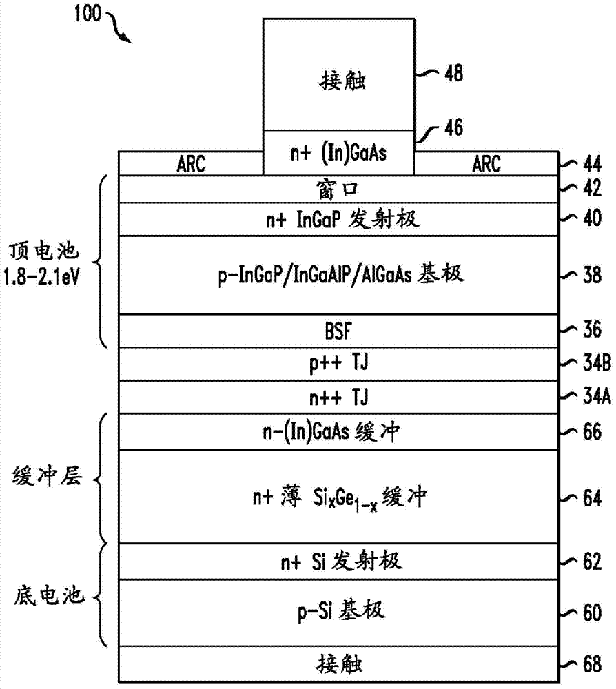
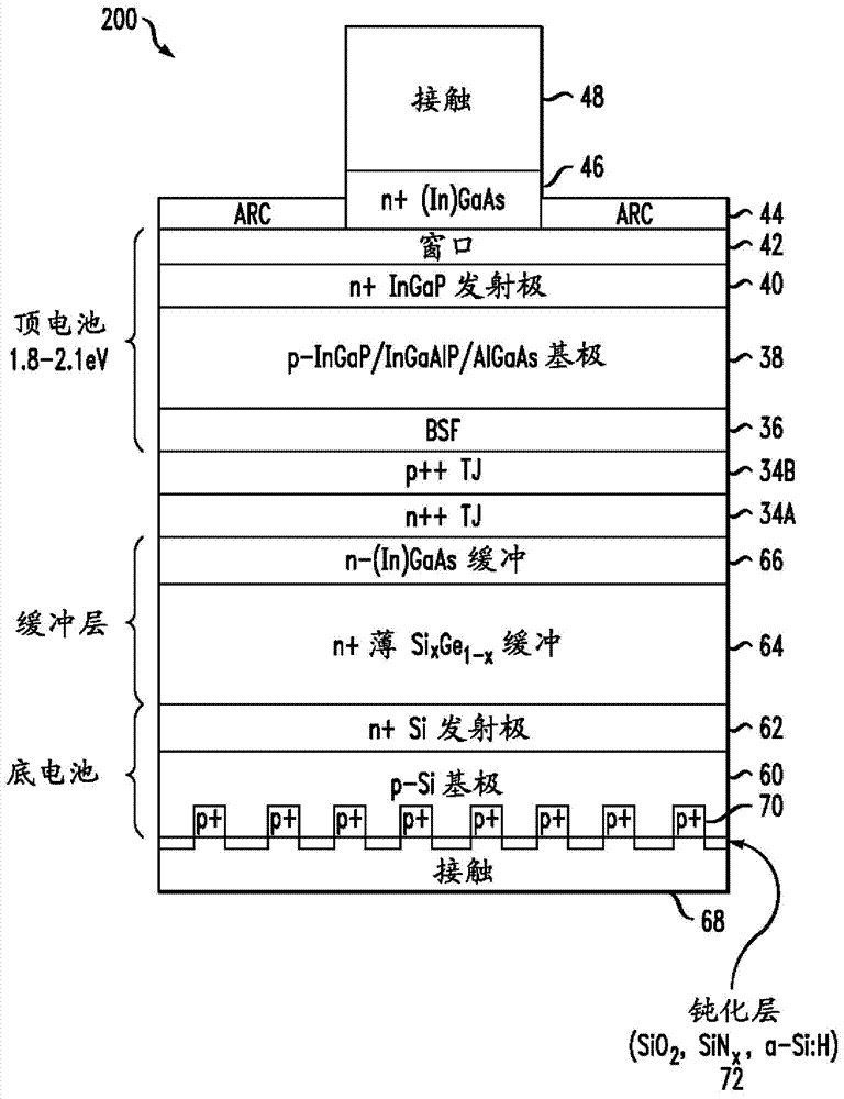
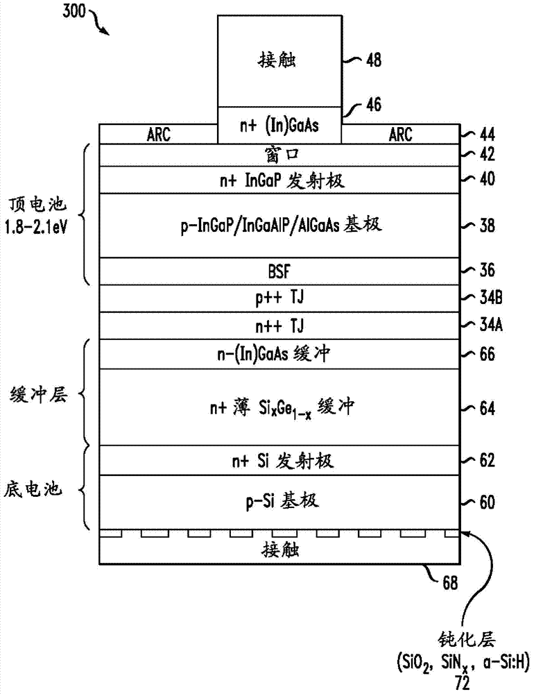
[0020] A germanium lattice-matched or pseudomorphic germanium multijunction III-V solar cell structure on a compliant silicon substrate is disclosed, in which silicon is used as the bottom cell. Growing III-V based cells on silicon is advantageous for a number of reasons including: (1) the abundance of Si substrates, (2) the lower cost of silicon compared to germanium and III-V semiconductor materials, ( 3) Mechanical stability, and (4) Silicon has the best bandgap for fabricating high-efficiency tandem junction solar cells. Lattice mismatch between silicon and III-V semiconductor materials is an obstacle to the realization of III-V solar cells on tandem silicon, where silicon serves as the bottom junction. Due to the challenging nature of growing III-V semiconductor materials directly on silicon over large areas as opposed to small patterned areas, researchers have attempted to use graded SiGe buffer layers as templates for growing III-V on silicon substrates. In principle a...
PUM
 Abstract
Description
Claims
Application Information
 - R&D Engineer
- R&D Manager
- IP Professional
- Industry Leading Data Capabilities
- Powerful AI technology
- Patent DNA Extraction
Browse by: Latest US Patents, China's latest patents, Technical Efficacy Thesaurus, Application Domain, Technology Topic, Popular Technical Reports.
© 2024 PatSnap. All rights reserved.Legal|Privacy policy|Modern Slavery Act Transparency Statement|Sitemap|About US| Contact US: help@patsnap.com