Circuit board manufacturing method

A manufacturing method and circuit board technology, applied in the directions of printed circuit manufacturing, printed circuits, printed circuits, etc., can solve the problems of easy residual air bubbles, easy formation of plug hole depressions, affecting detection and repair efficiency, etc. The effect of eliminating hidden quality hazards and reducing the risk of failure

Inactive Publication Date: 2014-07-23
DONGGUAN SHENGYI ELECTRONICS
View PDF1 Cites 22 Cited by
  • Summary
  • Abstract
  • Description
  • Claims
  • Application Information

AI Technical Summary

Problems solved by technology

However, this method has quality problems in practical application. For example, ① when filling the metallized hole with anti-corrosion material, it is easy to form a plug hole depression, which may expose part of the hole copper. The pad at the end of the hole will also etch away part of the copper on the hole wall, causing the etching depth to exceed the standard; ②During the process of plugging the hole, air bubbles are likely to remain in the anti-corrosion material, and when the air bubbles at the hole are close to the copper on the hole wall, it is easy to hide the potion , there is a risk of failure due to long-term erosion of the copper on the hole wall; ③ If there is resin residue after the ceramic grinding plate, residual copper in the hole is easy to appear after etching, resulting in failure of the insulation of the printed board via hole. In order to ensure zero defects in the product manufacturing process, After the circuit board etching is completed, AOI detection (that is, the detection of residual copper in the hole) is required. However, since the circuit board is usually placed for a period of time, the copper on the board surface is easy to oxidize and darken, which reduces the contrast between the copper and the substrate surface, resulting in defects. The problem of underreporting, so the AOI workshop is generally equipped with a pickling and deoxidation line to remove the oxide layer on the copper surface to enhance the contrast between the copper and the substrate. However, the circuit board contains CaCO in the plugging resin. 3 Composition, pickling will cause the resin to fall off and expose the copper in the hole, which will interfere with the detection process and cause many false points in the detection process, which will affect the efficiency of detection and repair

Method used


Image

  • Circuit board manufacturing method
  • Circuit board manufacturing method
  • Circuit board manufacturing method

Examples


Embodiment Construction

[0052] The technical solutions of the present invention will be further described below in conjunction with the accompanying drawings and through specific implementation methods.

[0053] Embodiments of the present invention provide a method for manufacturing a circuit board, comprising the following steps:

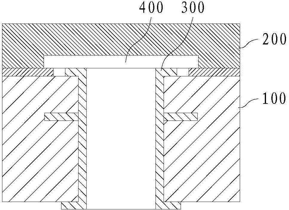
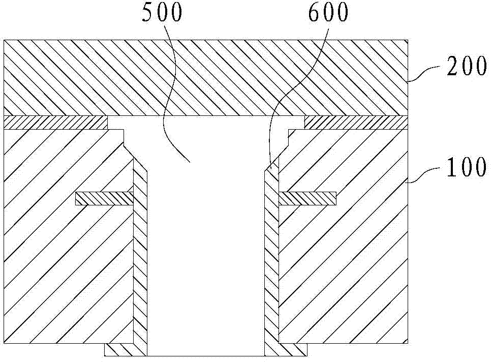
[0054] Step S10: providing a cover plate, opening a through hole corresponding to the metallized hole formed on the circuit board through electroplating on the cover plate, the aperture of the through hole is larger than the aperture of the metallized hole, so that the The cover plate covers the surface of the circuit board after electroplating, and the through hole is opposite to the metallized hole of the circuit board;

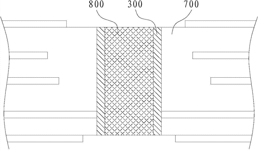
[0055] Step S20: providing a resin material with good wettability with the copper surface, so that the resin is fully stirred under vacuum conditions;

[0056] Step S30: Coating the stirred resin on the surface of the cover plate, the scraper of the s...


PUM


Abstract

The invention discloses a circuit board manufacturing method. The circuit board manufacturing method comprises the following steps of providing a cover plate, correspondingly forming a through hole corresponding to a plated-through hole of a circuit board in the cover plate and enabling the cover plate to cover the electroplated circuit board surface, wherein the through hole is aligned to the plated-through hole of the circuit board; providing a resin material with good copper face wettability and enabling the resin to be fully stirred under the vacuum condition; enabling the stirred resin to be coated on the cover plate surface, enabling the through hole of the cover plate to be full of the resin through a single stroke of a scraper of a silk-screen machine, wherein the rein flows into the plated-through hole through the through hole, and an oil return knife scrapes back the resin left on the cover plate surface; covering a pattern electrotinning layer on a electro-coppering layer required to be reserved, protecting patterns required to be reserved, enabling a copper ring at the hole opening position at at-least one end of the plated-through hole to be exposed, adopting alkaline etching liquid to perform etching to remove the copper ring protected by a tin-free layer, and performing etching for desired depth. The circuit board manufacturing method can remove the copper ring at the hole opening position of the plated-through hole, achieve through hole insulativity of the circuit board and effectively take the place of a backdrill technology.

Description

technical field [0001] The invention relates to the technical field of circuit board manufacturing, and more particularly relates to a circuit board manufacturing method capable of realizing through-hole insulation. Background technique [0002] A printed circuit board (PCB) is the provider of electrical connections for electronic components. PCB board metallized hole technology is one of the keys to printed circuit board manufacturing technology. Metallized hole refers to plating a thin layer of copper on the inner wall of the hole with a chemical reaction on the hole wall between the top layer and the bottom layer of the PCB board. , so that the top layer and the bottom layer of the PCB board are connected to each other. For some wireless communication products mounted with metallized structural parts, in order to ensure the reliability of product insulation, the earliest method is to slot the metal structural parts to process components. Please refer to figure 1 As sho...

Claims


Application Information

Patent Timeline
Patent Type & Authority Applications(China)
IPC IPC(8): H05K3/00H05K3/42
CPCH05K3/0094H05K3/425H05K2201/09563H05K2201/0959
Inventor 郭翔唐海波袁继旺
Owner DONGGUAN SHENGYI ELECTRONICS
Why Eureka
Try Eureka