
Eureka
For R&D, Eureka makes reading and utilizing patents & technical documents easy.
Eureka AIR
Designed for self-driven R&D workflows. Generate viable solutions, solve complex R&D challenges, empower your innovation with AI.

Eureka Materials
Designed for material experts only. Revolutionize your material R&D, from search, analyze, to developing new materials.

TechResearch
Generate reliable direction feasibility study reports for your R&D in just a few steps.

TechSeek
Discover and master advanced knowledge NOW. Basics, ideas, possibilities, all at once.

TechMind
As an expert in R&D Theories, TechMind can generates customized viable solutions instantly.

TechRisk
Analyze your overall solution with one click, know your potential R&D risks in advance.

TechMonitor
Get weekly tech updates, stay abreast of the latest tech innovations and key insights.
Optoelectronic sensor system
A photoelectric sensor, sensor layer technology, applied in fluorescence/phosphorescence, material excitation analysis, etc., can solve problems such as high cost, hindering miniaturization, and hindering the manufacture of reading systems
- Summary
- Abstract
- Description
- Claims
- Application Information
AI Technical Summary
Problems solved by technology
Method used
Image

Examples
Embodiment Construction
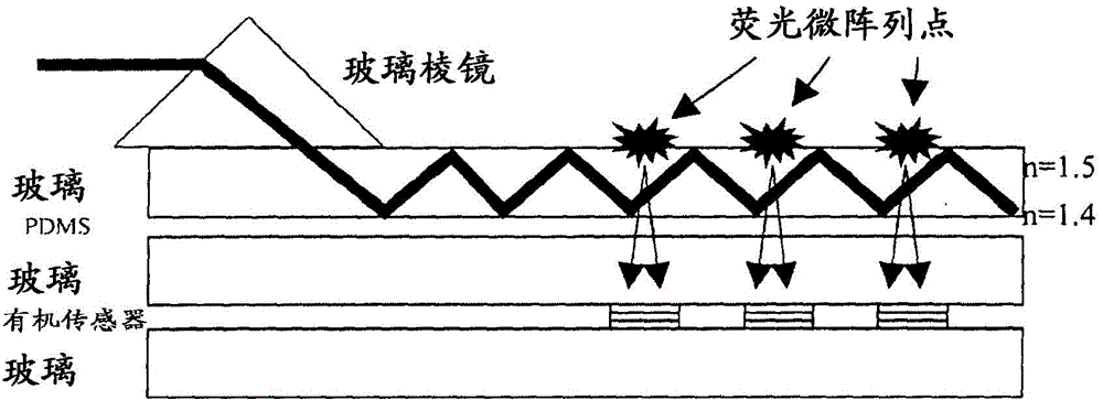
[0033] The incident angle of light rays entering the first glass carrier is preferably greater than the critical angle of total reflection between glass and PDMS, ie greater than 69°. (Refractive index: glass: n1=1.52, PDMS: n2=1.42->total reflection angle: α=arcsin(n2 / n1)=69.1°)
[0034] A photoelectric sensor system with this structure is characterized by the small size of this photoelectric sensor system, that is, the thickness of the first glass carrier can be, for example, 50 μm-200 μm, the thickness of the first glass carrier and the third glass carrier and the PDMS interlayer For example, it can be approximately 300 μm, and the overall thickness of the sensor can be, for example, approximately 1 mm.
[0035] The light source for excitation can be a laser, LED or OLED with a wavelength of 300nm-650nm.
PUM
| Property | Measurement | Unit |
|---|---|---|
| thickness | aaaaa | aaaaa |
| thickness | aaaaa | aaaaa |
| thickness | aaaaa | aaaaa |
Abstract
Description
Claims
Application Information
 - R&D Engineer
- R&D Manager
- IP Professional
- Industry Leading Data Capabilities
- Powerful AI technology
- Patent DNA Extraction
Browse by: Latest US Patents, China's latest patents, Technical Efficacy Thesaurus, Application Domain, Technology Topic, Popular Technical Reports.
© 2024 PatSnap. All rights reserved.Legal|Privacy policy|Modern Slavery Act Transparency Statement|Sitemap|About US| Contact US: help@patsnap.com