

Image sensor module and forming method thereof
An image sensor and image sensing technology, which is applied in radiation control devices and other directions, can solve the problems that the performance of image sensor modules needs to be improved, and achieve the effects of superior structural performance, reduced design difficulty, and improved packaging performance
- Summary
- Abstract
- Description
- Claims
- Application Information
AI Technical Summary
Problems solved by technology
Method used
Image

Examples
Embodiment Construction
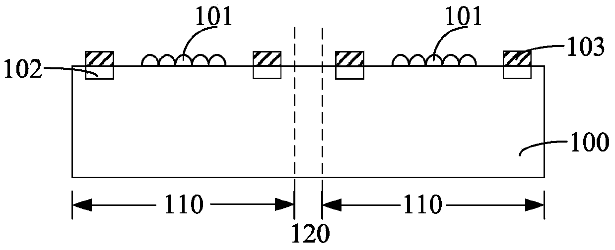
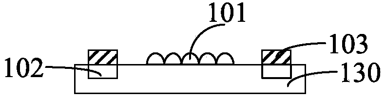
[0055] It can be seen from the background art that the existing chip packaging including the image sensing unit and the signal processing unit is difficult, and the performance of the formed image sensor module needs to be improved.
[0056] After research, it is found that in the prior art, the image sensing unit and the signal processing unit are usually packaged on the same chip. Specifically, the arrangement and interaction between the two should be considered when forming the signal processing chip on the image sensing chip. Connecting is a relatively difficult technology, which will lead to an increase in the difficulty of the packaging process; at the same time, the cost of the image sensor chip is high. After the signal processing chip is set on the image sensor chip, in order to consider the relationship between the signal processing chip and The interconnection of the image sensor chip will inevitably increase the area of the image sensor chip, resulting in a signif...
PUM
 Abstract
Description
Claims
Application Information