JFET (junction field-effect transistor) device and manufacturing method thereof

A device and condition technology, applied in semiconductor/solid-state device manufacturing, semiconductor devices, electrical components, etc., can solve the problems of low cost, can not well meet the application of constant current source circuit, etc., achieve small constant current accuracy, constant current good effect

Inactive Publication Date: 2014-08-06
UNIV OF ELECTRONICS SCI & TECH OF CHINA
View PDF4 Cites 0 Cited by
  • Summary
  • Abstract
  • Description
  • Claims
  • Application Information

AI Technical Summary

Problems solved by technology

Its driving circuit has a simple structure and extremely low cost, and the core of providing constant current is a normally-on n-channel JFET device, but the current conventional JFET device cannot well meet the application of constant current source circuit

Method used


Image

  • JFET (junction field-effect transistor) device and manufacturing method thereof
  • JFET (junction field-effect transistor) device and manufacturing method thereof
  • JFET (junction field-effect transistor) device and manufacturing method thereof

Examples


Embodiment 1

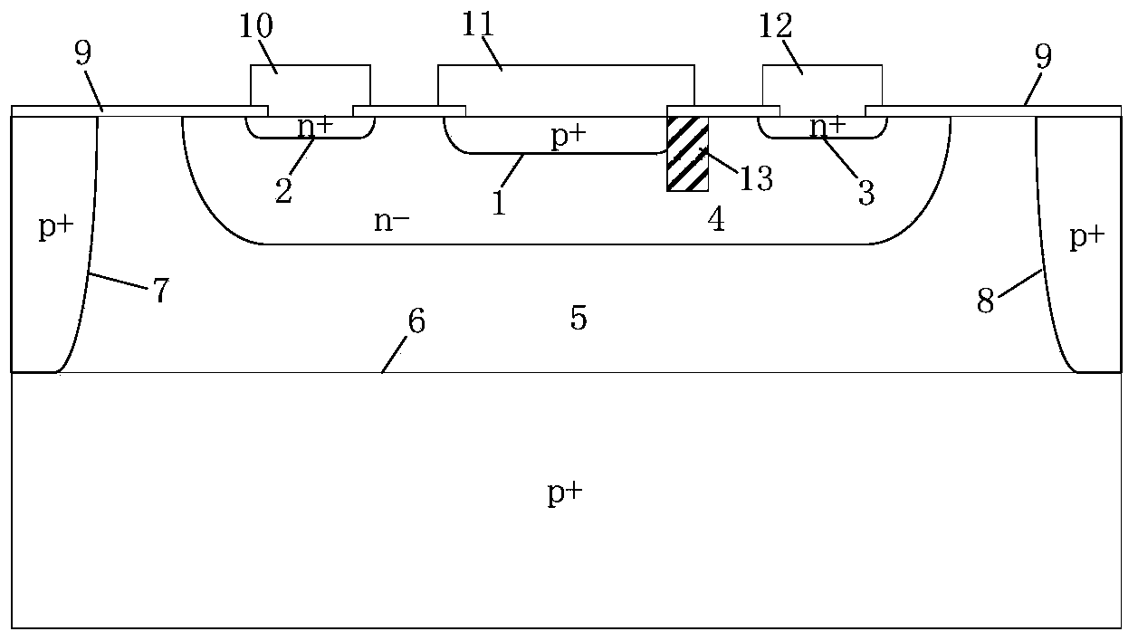
[0038] In this example, a shallow trench auxiliary layer is formed by digging a trench and filling a dielectric material layer, specifically:

[0039] Step 1: Select an NTD monocrystalline silicon wafer with a thickness of about 400-700 μm and a resistivity of 0.001-0.005Ω·cm;

[0040] Step 2: growing a P-type epitaxial layer 5 on the surface of the silicon wafer, the growth condition is a temperature of 1100°C-1150°C, the thickness of the P-type epitaxial layer 5 is 5-25 μm, and the resistivity is 8-12Ω·cm;

[0041] Step 3: Thermally grow oxide layer with a thickness of

[0042] Step 4: Form a first P-type isolation region 7 and a second P-type isolation region 8 on both sides of the P-type epitaxial layer 5 by photolithography and ion implantation, specifically: grow 40-100nm thick before ion implantation The oxide layer, ion implantation after photolithography, ion implantation conditions: dose 1e15 ~ 8e15cm -2 , Energy 40~80KeV, redistribution condition: anaerobic cond...


PUM


Abstract

The invention relates to semiconductor technology, particularly a JFET (junction field-effect transistor) device and a manufacturing method thereof. A shallow groove auxiliary layer 13 is introduced to one end of a gate region of the JFET device and is adjacent to the side of the source end; and thus, the shallow groove auxiliary layer 13 is utilized to reduce the ditch modulation effect, thereby implementing small variable rate within wide voltage input range. The device has favorable constant-current characteristic on the basis of uncomplex manufacturing technique, has small variable rate within wide voltage input range, can satisfy the demand for lower constant-current precision, and is especially suitable for low-power LED (light-emitting diode) lamp constant-current drive. The method is especially suitable for low-power LED lamp constant-current JFET devices.

Description

technical field [0001] The invention relates to semiconductor technology, in particular to a JFET device and a manufacturing method thereof. Background technique [0002] With the widespread use of LED lamps, LED constant current drivers are rapidly occupying the market. The constant current JFET device is a constant current driver designed for low-power LEDs. It can achieve constant current output in a wide voltage range from 4V to 150V, and It can achieve ±15% constant current accuracy, can be matched with LED lamp beads, and is widely used in indoor lighting. figure 1 It is a solution for driving LEDs with constant current. Due to the high output voltage, this solution is especially suitable for LED applications with a current value of 5mA to 500mA, especially for high-voltage LEDs. The scheme includes a total of 6 components, simple and practical, and low cost. figure 1 Among them, the AC mains directly drives the constant current device and the LED light string after ...

Claims


Application Information

Patent Timeline
Patent Type & Authority Applications(China)
IPC IPC(8): H01L29/808H01L21/337
CPCH01L29/808H01L29/1058H01L29/66893
Inventor 李泽宏赖亚明刘建弋才敏吴玉舟伍济
Owner UNIV OF ELECTRONICS SCI & TECH OF CHINA
Why Eureka
Try Eureka