Barrel type furnace and method for manufacturing semiconductor

A barrel-type, cavity technology, applied in semiconductor/solid-state device manufacturing, electrical components, circuits, etc., can solve the problems of low product yield, uneven resistivity and thickness of epitaxial layers, etc., to improve product yield, The effect of uniform thickness and resistivity

Inactive Publication Date: 2014-08-13
ADVANCED SEMICON MFG CO LTD
View PDF3 Cites 2 Cited by
  • Summary
  • Abstract
  • Description
  • Claims
  • Application Information

AI Technical Summary

Problems solved by technology

[0006] The purpose of the present invention is to provide a barrel furnace and a semiconductor manufacturing method to solve the problem that the epitaxial layer often appears on the substrate carried by the upper zone and the lower zone after the epitaxial process is performed using the barrel furnace in the prior art. The phenomenon that the resistivity and thickness are not very uniform leads to the problem of low product yield

Method used


Image

  • Barrel type furnace and method for manufacturing semiconductor
  • Barrel type furnace and method for manufacturing semiconductor
  • Barrel type furnace and method for manufacturing semiconductor

Examples


Embodiment Construction

[0034] The barrel furnace proposed by the present invention will be described in further detail below in conjunction with the accompanying drawings and specific embodiments. Advantages and features of the present invention will be apparent from the following description and claims. It should be noted that all the drawings are in a very simplified form and use imprecise scales, and are only used to facilitate and clearly assist the purpose of illustrating the embodiments of the present invention.

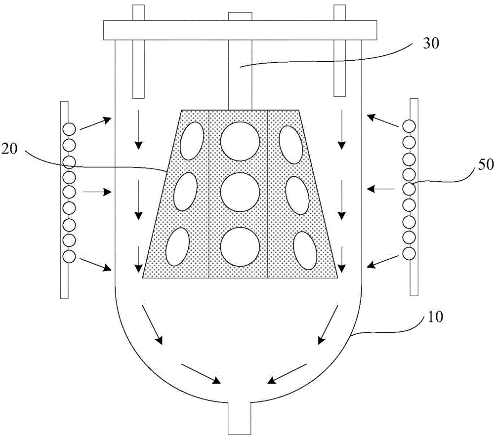
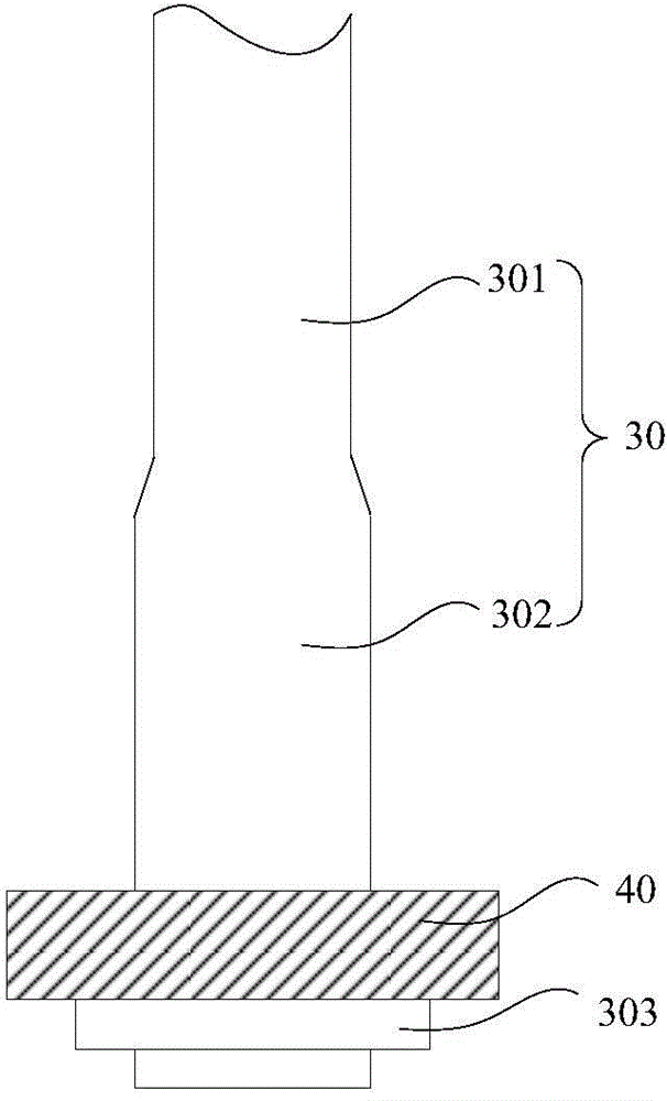
[0035] Please refer to figure 1 and figure 2 ,in, figure 1 It is the front view of the barrel furnace in an embodiment of the present invention, figure 2 It is a structural schematic diagram of a detachable gasket provided on the suspender in the barrel furnace. Such as figure 1 As shown, the barrel furnace suitable for the epitaxial process includes: a cavity 10, a base 20 disposed in the cavity 10, a suspension mounted on the base 20 and connected to the cavity 10 Rod 30; w...


PUM


Abstract

The invention provides a barrel type furnace and a method for manufacturing a semiconductor. The barrel type furnace is suitable for the epitaxy technique, the length of a suspender is set to be 300 mm to 350 mm, the suspender is used in cooperation with detachable gaskets, the number of the gaskets on the suspender is increased or reduced according to actual needs, the vertical position of a base in the vertical direction can be adjusted, substrates borne by an upper area and a lower area are located in a good temperature control area when the epitaxy technique is carried out, and therefore after the epitaxy technique is carried out, epitaxial layers on the substrates are even in thickness and electrical resistivity, and the product yield is improved.

Description

technical field [0001] The invention relates to the technical field of semiconductor manufacturing, in particular to a barrel furnace and a semiconductor manufacturing method. Background technique [0002] The epitaxial process refers to the growth of a single crystal layer on a single crystal substrate, and the newly grown layer is called an epitaxial layer. The epitaxial process is divided into two types: homoepitaxial and heteroepitaxial. Homoepitaxy means that the epitaxial layer is made of the same material as the substrate, such as epitaxial silicon on a silicon substrate. Hetero-epitaxy means that the epitaxial layer is inconsistent with the substrate material, such as epitaxial alumina on a silicon substrate. The epitaxy process is widely used in the manufacture of bipolar devices, CMOS, silicon-based BiCMOS, germanium-silicon BiCMOS and BCD devices. For mass production of these devices, the core problem to be solved is the control of product parameters, which req...

Claims


Application Information

Patent Timeline
Patent Type & Authority Applications(China)
IPC IPC(8): H01L21/67H01L21/02
CPCH01L21/6719H01L21/02617
Inventor 苏建培张健丁海东
Owner ADVANCED SEMICON MFG CO LTD
Why Eureka
Try Eureka