A vacuum brazing chip mounting process method without load and low void ratio

A process method and low-void technology, applied in auxiliary devices, manufacturing tools, welding equipment, etc., can solve the problems of large void rate in chip loading, demanding chip requirements, easy to damage chips, etc., to improve brazing quality and yield , Reduce the brazing void rate, improve the effect of brazing quality

Active Publication Date: 2016-01-13
BEIJING MXTRONICS CORP +1
View PDF4 Cites 0 Cited by
  • Summary
  • Abstract
  • Description
  • Claims
  • Application Information

AI Technical Summary

Problems solved by technology

[0002] At present, in integrated circuit packaging, the size of the chip mounted by soldering is usually less than 10mm×10mm. During the process of soldering the chip, it is necessary to use a load such as a pressure block to provide the downward force of the chip, so that the chip, the soldering piece and the shell substrate are in contact. It is more compact, which inevitably makes the contact between the pressing block and the chip surface, whether it is "point" contact or "surface" contact, which puts forward high requirements on the cleanliness of the chip surface. However, the tiny silicon powder and silicon slag on the chip surface will The chip is damaged under the action of the pressing block, and the surface of the pressing block is easy to be stained after repeated use, and it will cause a large void rate inside the chip, which seriously affects the yield of the brazing chip, and the requirements for the chip are too harsh. As a result, some chips that are extremely prone to damage cannot be soldered and mounted

Method used


Image

  • A vacuum brazing chip mounting process method without load and low void ratio
  • A vacuum brazing chip mounting process method without load and low void ratio
  • A vacuum brazing chip mounting process method without load and low void ratio

Examples


Embodiment 1

[0027] Step (1), solder selection

[0028] The sizes of the chips to be brazed are 1mm×1mm, 5mm×5mm, 10mm×10mm, respectively, and Au80Sn20 solder is selected.

[0029] Step (2), metallization on the back of the chip

[0030] The back of the chip to be brazed is metallized by sputtering Au process.

[0031] Step (3), film loading

[0032] Install the chip to be brazed on the gold-plated chip area to be brazed on the integrated circuit package shell, and put Au80Sn20 solder between the chip to be soldered and the gold-plated chip area to be brazed;

[0033] Step (4), place the sample to be welded in vacuum brazing equipment for brazing, the specific process is as follows:

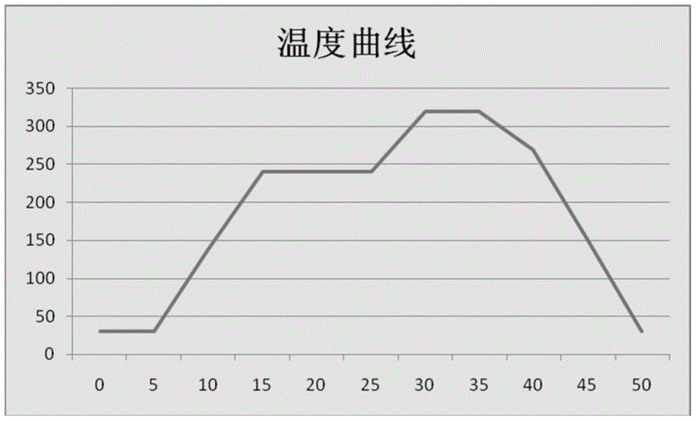
[0034] (1) From room temperature (generally 15-30°C) to 180°C, the heating rate is 1°C / s, and the temperature is kept for 4 minutes;

[0035] (2), continue to heat up to 220 ° C, the heating rate is 1 ° C / s, vacuumize, so that the vacuum in the brazing equipment is reduced to <0.001mbar;

[0036] (3), ...

Embodiment 2

[0043] Step (1), solder selection

[0044] The size of the chip to be brazed is 1mm×1mm, 5mm×5mm, 10mm×10mm respectively, and Pb92.5Sn2.5Ag5 solder is selected.

[0045] Step (2), metallization on the back of the chip

[0046] The back of the chip to be brazed is metallized by sputtering Au process.

[0047] Step (3), film loading

[0048] The chip to be brazed is installed in the gold-plated area to be brazed of the integrated circuit package shell, and Pb92.5Sn2.5Ag5 solder is put between the chip to be soldered and the gold-plated area to be brazed;

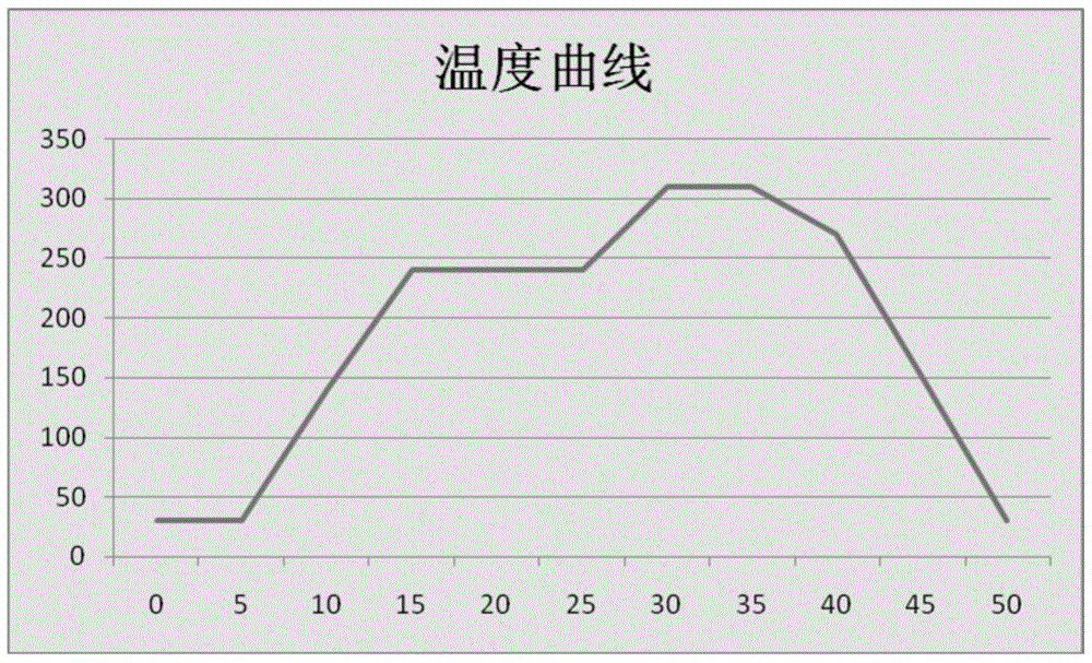
[0049] Step (4), place the sample to be welded in vacuum brazing equipment for brazing, the specific process is as follows:

[0050] (1) From room temperature to 176°C, the heating rate is 1.5°C / s, and the temperature is kept for 5 minutes;

[0051] (2) Continue to heat up to 218°C with a heating rate of 1.5°C / s, and vacuumize to reduce the vacuum in the brazing equipment to <0.001mbar;

[0052] (3), continue to heat up t...


PUM


Abstract

The invention relates to a low-voidage vacuum brazing chip mounting technique free of loads. The technique comprises the following steps that (1), a sputtering Au technology is adopted in the back face of a chip to be brazed, and the back face is metallized; (2), the chip to be brazed is arranged on a to-be-brazed gold plating chip mounting area of an integrated circuit packaging shell, and brazing materials are placed between the chip to be brazed and the to-be-brazed gold plating chip mounting area; (3), a test sample to be brazed is placed in brazing equipment to be brazed according to technological conditions specially designed. In the brazing process, temperature curve optimization is combined with vacuum degree control, the air pressure difference is used for replacing the pressing block loads, optimization design is carried out on the temperature interval, the heating rate, the heat preservation time and the vacuum degree, the optimal technological conditions are determined, the problem that the chip is damaged due to adopted loads in the traditional method is solved, the brazing voidage is lowered, and the brazing yield and brazing quality are obviously improved.

Description

technical field [0001] The invention belongs to the technical field of semiconductor ceramic packaging technology, and in particular relates to a vacuum brazing chip loading process method without load and low void ratio. Background technique [0002] At present, in integrated circuit packaging, the size of the chip mounted by soldering is usually less than 10mm×10mm. During the process of soldering the chip, it is necessary to use a load such as a pressure block to provide the downward force of the chip, so that the chip, the soldering piece and the shell substrate are in contact. It is more compact, which inevitably makes the contact between the pressing block and the chip surface, whether it is "point" contact or "surface" contact, which puts forward high requirements on the cleanliness of the chip surface. However, the tiny silicon powder and silicon slag on the chip surface will The chip is damaged under the action of the pressing block, and the surface of the pressing ...

Claims


Application Information

Patent Timeline
Patent Type & Authority Patents(China)
IPC IPC(8): B23K1/00B23K3/08
CPCB23K1/00B23K3/08
Inventor 冯小成荆林晓练滨浩曹玉生贺晋春陈宪荣陈建安姚全斌
Owner BEIJING MXTRONICS CORP
Why Eureka
Try Eureka