Pixel circuit and driving method, organic light-emitting diode (OLED) display panel and device thereof

A technology of pixel circuit and display panel, applied in the field of OLED display, can solve the problems of current inconsistency, increase in cost, decrease in aperture ratio, etc., and achieve the effects of reducing current density, prolonging service life, and increasing aperture ratio

Active Publication Date: 2014-09-10
BOE TECH GRP CO LTD
View PDF4 Cites 38 Cited by
  • Summary
  • Abstract
  • Description
  • Claims
  • Application Information

AI Technical Summary

Problems solved by technology

[0002] The OLED (Organic Light Emitting Diode, Organic Light Emitting Diode) panel can emit light is driven by the current generated by driving the TFT (Thin Film Transistor, Thin Film Field Effect Transistor) in the saturated state, because when the same gray scale voltage is input, different critical The voltage will produce different drive currents, resulting in current inconsistencies
For example, the brightness uniformity of the traditional 2T1C pixel drive circuit has been poor. At present, the solution is to add a compensation circuit in the pixel, and eliminate the influence of the threshold voltage Vth of the driving TFT through the compensation TFT circuit.
But the disadvantage is that the increase of TFT often leads to a rapid decrease in the aperture ratio and increases the cost. Under the same pixel driving current condition, although the brightness of the AMOLED panel with a low aperture ratio may not necessarily decrease, the current density of its organic light-emitting layer will inevitably increase. , which easily leads to the aging of the light-emitting layer material, and the service life of the entire OLED panel is reduced

Method used


Image

  • Pixel circuit and driving method, organic light-emitting diode (OLED) display panel and device thereof
  • Pixel circuit and driving method, organic light-emitting diode (OLED) display panel and device thereof
  • Pixel circuit and driving method, organic light-emitting diode (OLED) display panel and device thereof

Examples


Embodiment Construction

[0053] The following will clearly and completely describe the technical solutions in the embodiments of the present invention with reference to the accompanying drawings in the embodiments of the present invention. Obviously, the described embodiments are only some, not all, embodiments of the present invention. Based on the embodiments of the present invention, all other embodiments obtained by persons of ordinary skill in the art without making creative efforts belong to the protection scope of the present invention.

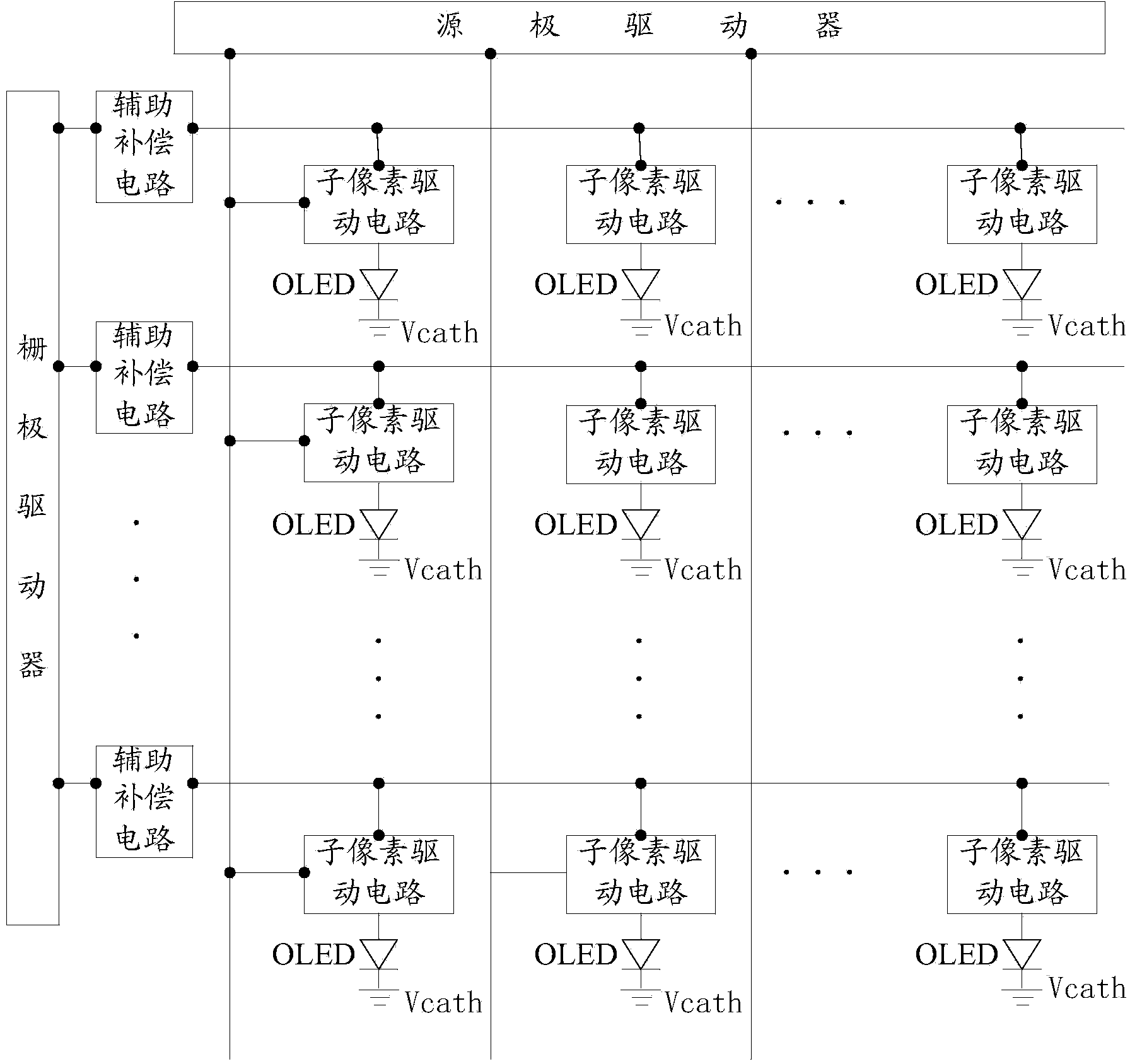
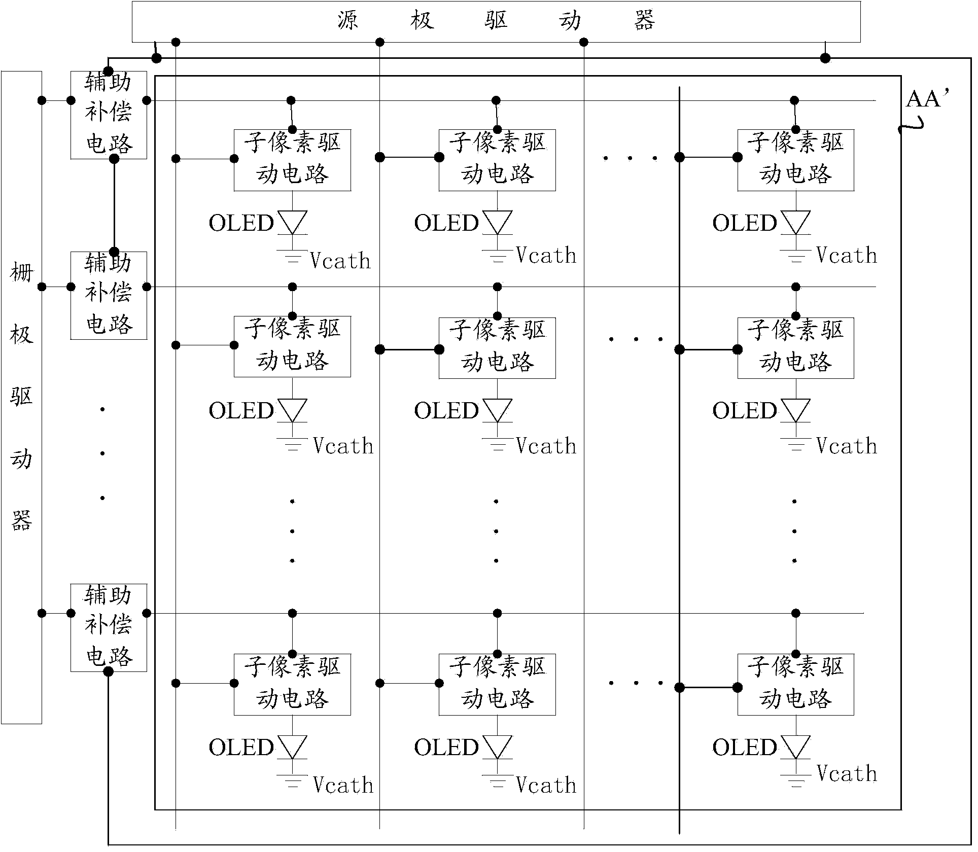
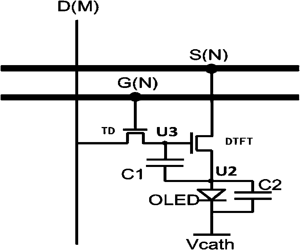
[0054] The pixel circuit described in the embodiment of the present invention is applied to an OLED display panel, and includes multiple rows of pixel units, each row of pixel units includes a plurality of sub-pixel units; each of the sub-pixel units includes a sub-pixel driving circuit and an OLED; the sub-pixel The drive circuit includes a drive transistor connected to the OLED, and a drive control module respectively connected to a data line and the drive tr...


PUM


Abstract

The invention provides a pixel circuit and a driving method, an organic light-emitting diode (OLED) display panel and a device thereof. The pixel circuit comprises a plurality of rows of pixel units. Each row of pixel units comprises a plurality of sub pixel units and further comprises an auxiliary compensation circuit. Each auxiliary compensation circuit generates a switch control signal input into a sub pixel driving circuit included by the corresponding sub pixel units according to a scanning signal from a gate drive circuit and generates a compensation control signal input to the sub pixel driving circuit according to a control signal from the gate drive circuit, and the sub pixel driving circuit receives data voltage from a data line according to the switch control signal, controls the OLED to emit light according to the data voltage through a driving transistor included by the sub pixel driving circuit, and controls and compensates threshold voltage of the driving transistor according to the compensation control signal when the driving transistor drives the OLED to emit light. By means of the pixel circuit, the driving method, the OLED display panel and the device, the pixel circuit design is simplified, the pixel opening rate is increased, the service life of the OLED panel is prolonged, and the cost is reduced.

Description

technical field [0001] The present invention relates to the field of OLED (Organic Light-Emitting Diode, Organic Light-Emitting Diode) display technology, in particular to a pixel circuit and a driving method thereof, an OLED display panel and an OLED display device. Background technique [0002] The OLED (Organic Light Emitting Diode, Organic Light Emitting Diode) panel can emit light is driven by the current generated by driving the TFT (Thin Film Transistor, Thin Film Field Effect Transistor) in the saturated state, because when the same gray scale voltage is input, different critical The voltage will produce different drive currents, causing current inconsistencies. For example, the brightness uniformity of the traditional 2T1C pixel driving circuit has always been poor. The current solution is to add a compensation circuit in the pixel, and eliminate the influence of the threshold voltage Vth of the driving TFT through the compensation TFT circuit. But the disadvantage...

Claims


Application Information

Patent Timeline
Patent Type & Authority Applications(China)
IPC IPC(8): G09G3/32G09G3/3208
CPCG09G3/3233G09G2300/0852G09G3/2074G09G3/3208G09G2320/045
Inventor 杨飞张晨吴月
Owner BOE TECH GRP CO LTD
Why Eureka
Try Eureka