LED flip chip manufacturing method and LED flip chip

An LED chip and flip-chip technology, applied in electrical components, circuits, semiconductor devices, etc., can solve the problems of reduced reflection efficiency, the inability of the metal reflection layer to take into account the reflectivity and conductivity, and the performance limitations of metal materials to improve luminous efficiency. Effect

Inactive Publication Date: 2014-09-10
EPITOP PHOTOELECTRIC TECH
View PDF7 Cites 32 Cited by
  • Summary
  • Abstract
  • Description
  • Claims
  • Application Information

AI Technical Summary

Problems solved by technology

[0005] The invention provides a method for preparing a flip-chip LED chip and a flip-chip LED chip to solve the problem that the flip-chip LED chips prepared in the prior art cannot balance refl

Method used


Image

  • LED flip chip manufacturing method and LED flip chip
  • LED flip chip manufacturing method and LED flip chip
  • LED flip chip manufacturing method and LED flip chip

Examples


preparation example Construction

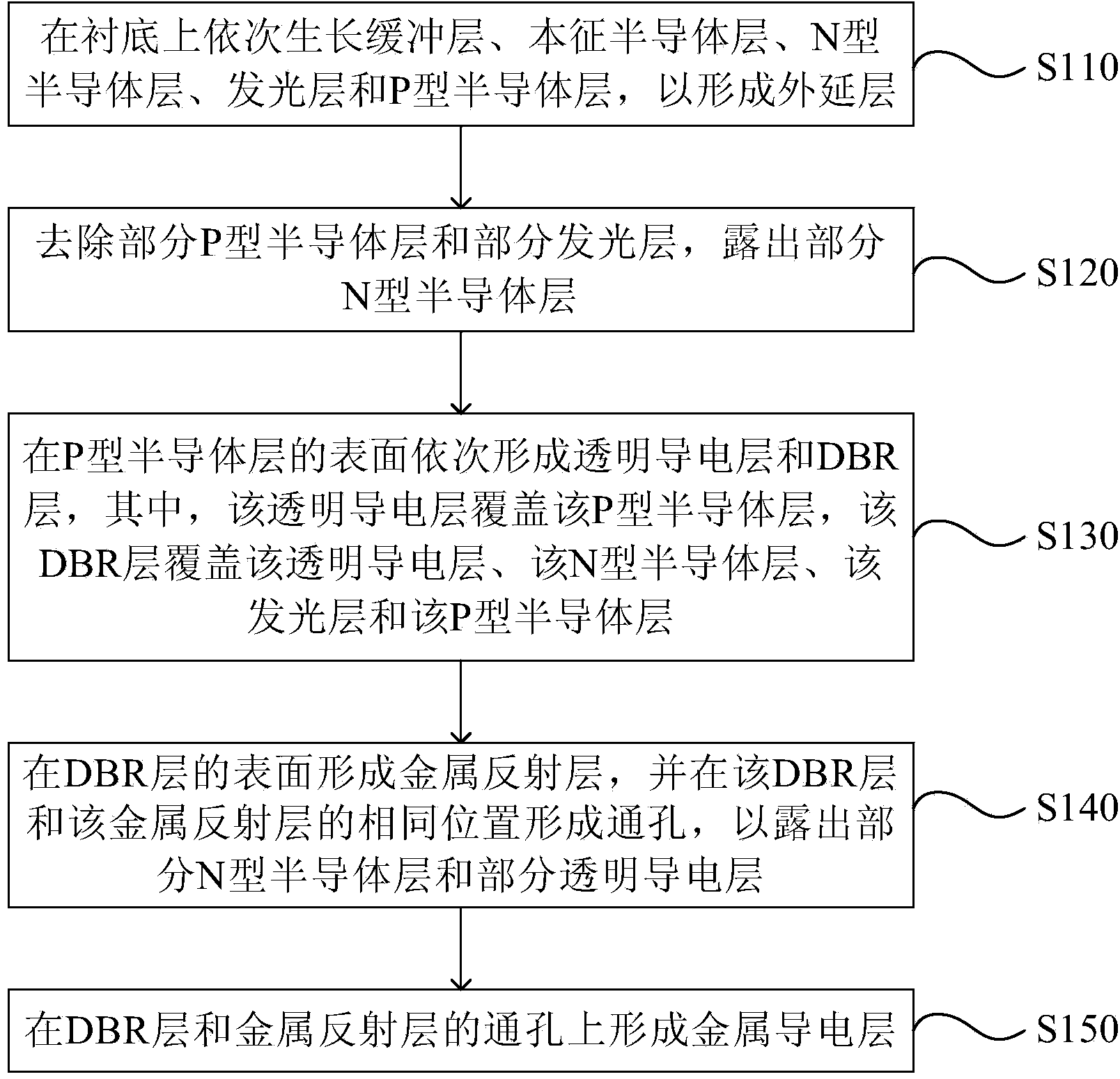
[0046] figure 1 It is a flowchart of an embodiment of a method for manufacturing a flip-chip LED chip provided by the present invention. Such as figure 1 As shown, the method of this embodiment may include:

[0047] S110, sequentially growing a buffer layer, an intrinsic semiconductor layer, an N-type semiconductor layer, a light-emitting layer, and a P-type semiconductor layer on the substrate to form an epitaxial layer.

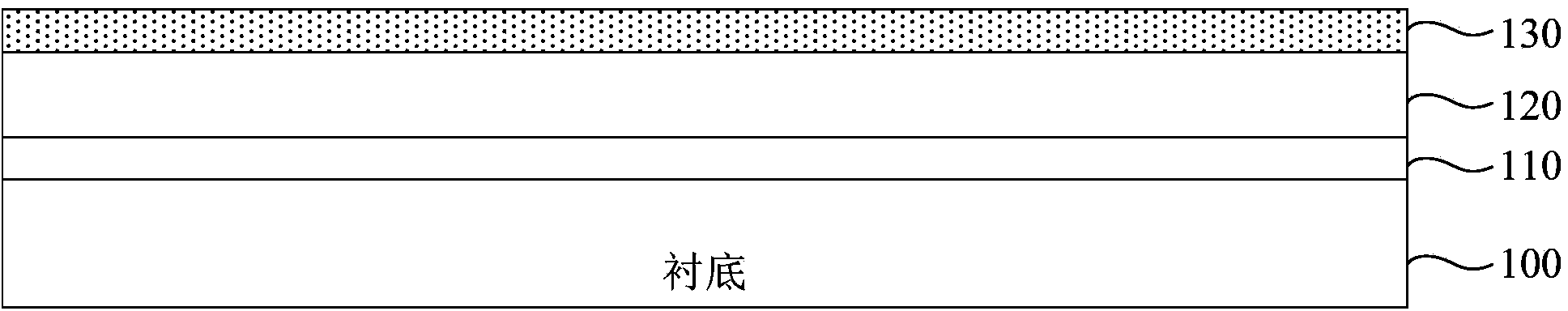
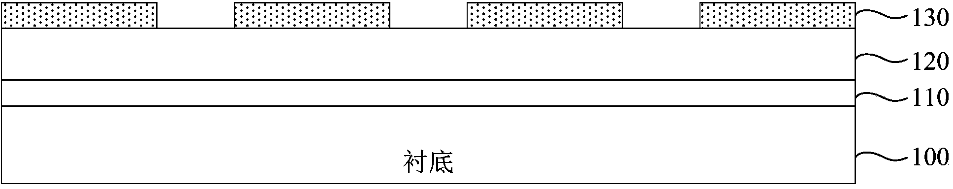
[0048] In the process of chip preparation, semiconductor wafers are usually used as the substrate material. In this embodiment, when preparing flip-chip LED chips, the sapphire commonly used as the substrate material is used as an example to illustrate, as shown in figure 2 shown, for figure 1 A schematic chip structure diagram of a manufacturing method of a flip-chip LED chip provided by the illustrated embodiment, in which a buffer layer 110, an intrinsic semiconductor layer (not shown in the figure), and an N-type semiconductor layer are sequentially...


PUM


Abstract

The invention provides an LED flip chip manufacturing method and an LED flip chip. The method includes the steps of sequentially growing a buffer layer, an intrinsic semiconductor layer, an N type semiconductor layer, a light-emitting layer and a P type semiconductor layer on a substrate so as to form an epitaxial layer, removing part of the P type semiconductor layer and part of the light-emitting layer to expose part of the N type semiconductor layer, sequentially forming a transparent conducting layer and a DBR layer on the surface of the P type semiconductor layer, forming a metal reflection layer on the surface of the DBR layer, forming through holes in the same positions of the DBR layer and the metal reflection layer to expose part of the N type semiconductor layer and part of the transparent conducting layer, and forming metal conducting layers on the through holes of the DBR layer and the through holes of the metal reflection layer. By means of the method, the problems that when the LED flip chip is manufactured based on the existing technology, due to the limitation of the performance of metal materials, the requirement for the reflection rate and the requirement for electrical conductivity can not be taken into consideration at the same time when the metal reflection layer is manufactured, and the reflection efficiency is lowered are solved.

Description

technical field [0001] The invention relates to chip manufacturing technology, in particular to a method for preparing a flip-chip LED chip and the flip-chip LED chip. Background technique [0002] With the development of light-emitting diode (Light Emitting Diode, referred to as: LED) technology, LED chips have been widely used in lighting, indication, display and backlight, because the flip-chip LED chip can avoid the light shielding of metal electrodes, through As a light-transmitting surface, the substrate increases the area of ​​the light-emitting area, and can take into account the advantages of the balance of light transmittance and square resistance, and has gradually replaced the traditional front-mounted LED chips. [0003] The current flip-chip LED chip usually forms a reflective layer on the epitaxial surface, which can reflect the light of the epitaxial layer to the substrate and emit it. The material of the reflective layer can be a metal with high reflectivity...

Claims


Application Information

Patent Timeline
IPC IPC(8): H01L33/00H01L33/46H01L33/38
CPCH01L33/0066H01L33/0075H01L33/38H01L33/46H01L2933/0016
Inventor 姚禹郑远志陈向东康建梁旭东
Owner EPITOP PHOTOELECTRIC TECH
Why Eureka
Try Eureka