All-inorganic SMD LED packaging method and structure

An LED packaging and inorganic technology, applied in electrical components, circuits, semiconductor devices, etc., can solve the problems of device luminous flux, radiant flux attenuation, difficulty in inorganic sealing packaging technology, poor UV resistance, etc., to improve heat dissipation performance and save energy. The cost of gold wire and the effect of strong anti-aging ability

An LED packaging and inorganic technology, applied in electrical components, circuits, semiconductor devices, etc., can solve the problems of device luminous flux, radiant flux attenuation, difficulty in inorganic sealing packaging technology, poor UV resistance, etc., to improve heat dissipation performance and save energy. The cost of gold wire and the effect of strong anti-aging ability

CN104037280AActive Publication Date: 2014-09-10厦门多彩光电子科技有限公司

Image

  • All-inorganic SMD LED packaging method and structure
  • All-inorganic SMD LED packaging method and structure
  • All-inorganic SMD LED packaging method and structure

Examples


Embodiment Construction

[0030] The present invention will be further described in conjunction with the accompanying drawings and specific embodiments.

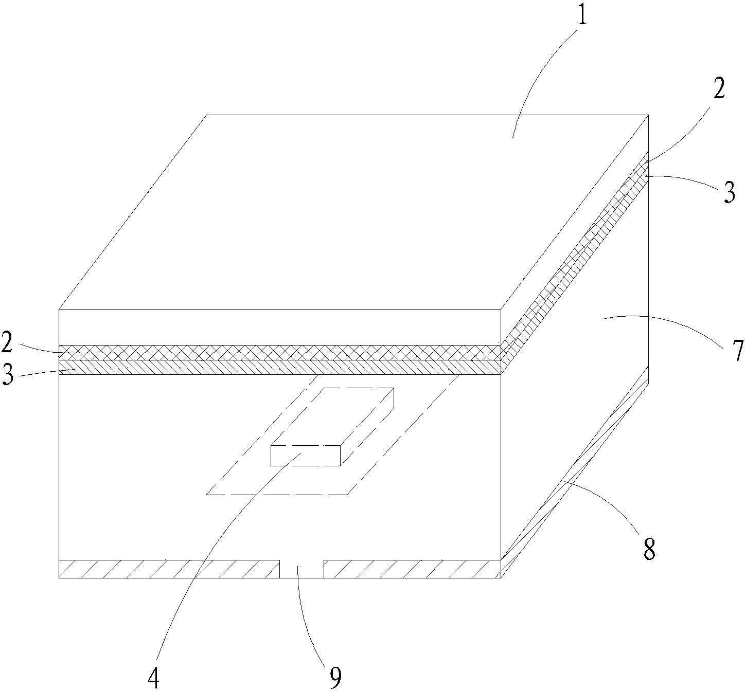
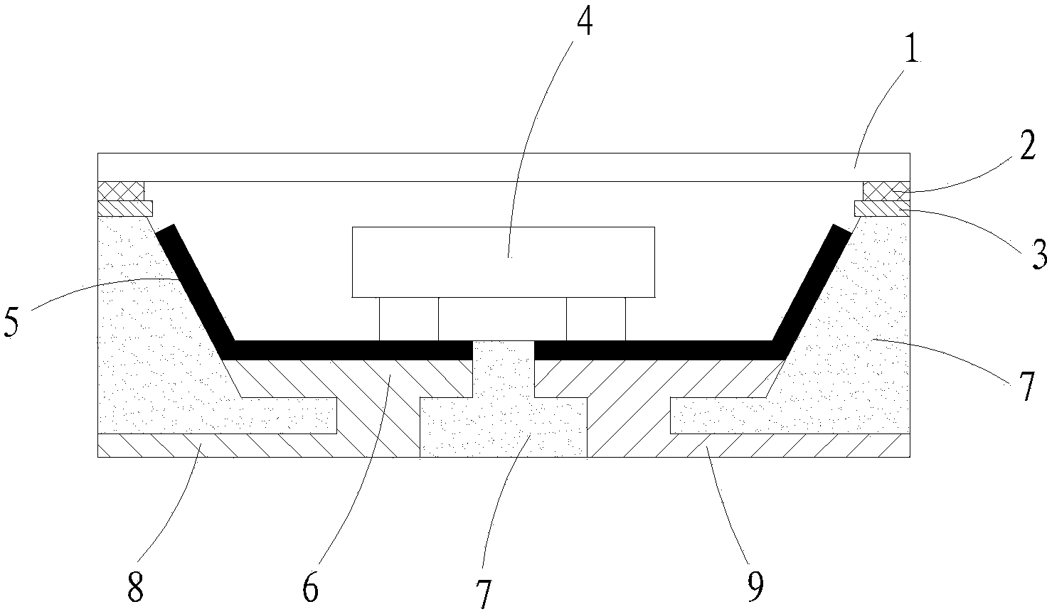
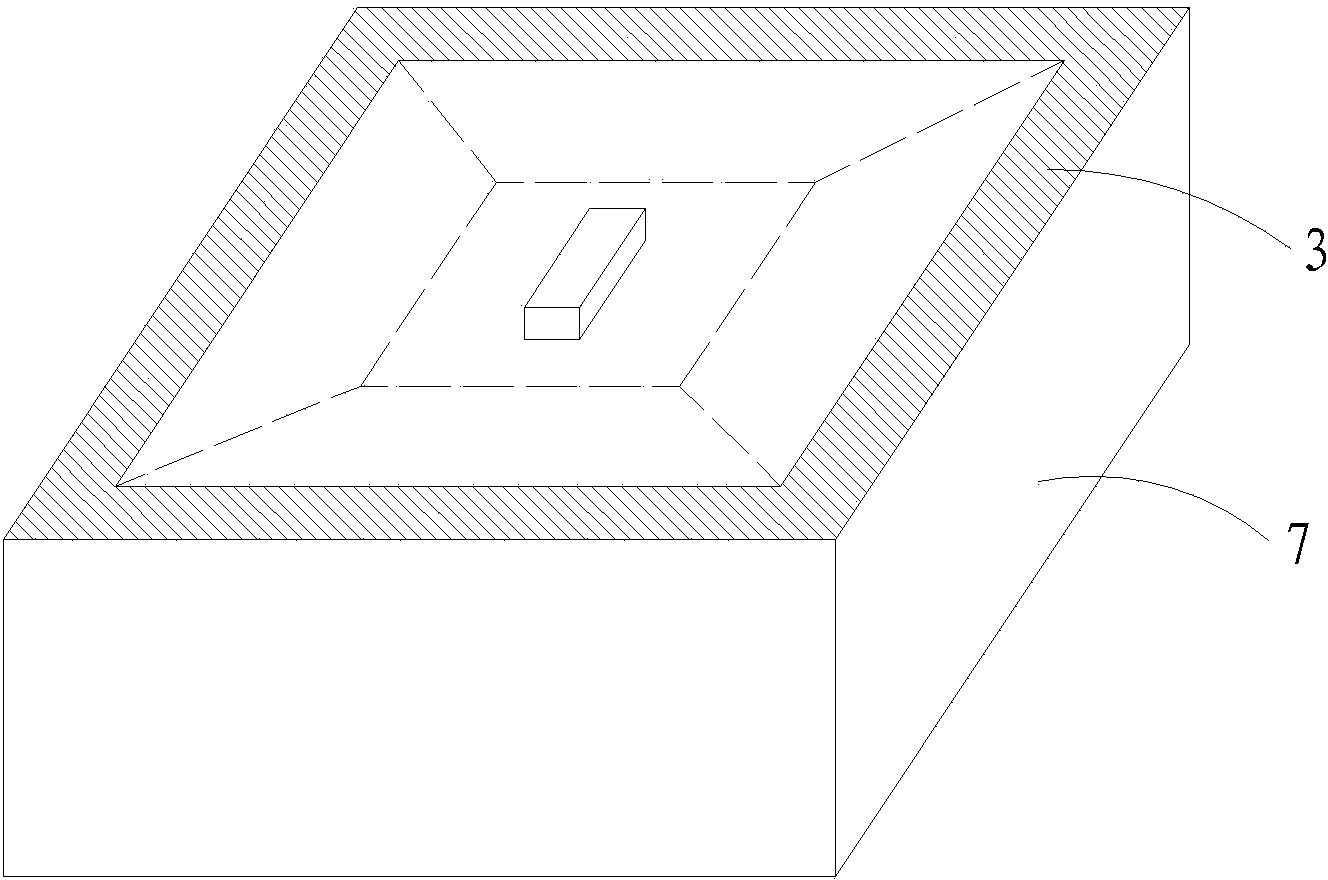
[0031]A kind of all-inorganic patch LED package structure of the present invention, see Figure 1-Figure 4 , including a bracket 7 made of a ceramic substrate, on which a glass cover 1 matching the structure of the bracket 7 is provided to just cover the bracket 7; Groove, the bracket 7 is provided with a first metal layer 3 along the periphery and at the peripheral position of the groove, the edge of the glass cover 1 is provided with a circle of second metal layer 2, and the expansion of the material of the second metal layer 2 The coefficient is similar to that of the glass cover plate, the materials of the first metal layer 3 and the second metal layer 2 have similar melting points and can be well welded, and the second metal layer 2 and the first metal layer 3 are connected together by resistance welding. The purpose of using the above-mentione...


PUM

PropertyMeasurementUnit
Total thicknessaaaaaaaaaa
Thicknessaaaaaaaaaa
Boiling pointaaaaaaaaaa

Abstract

The invention discloses an all-inorganic SMD LED packaging method. The method includes the following processes that firstly, a support is manufactured, secondly, dehumidification, baking and plasma cleaning are conducted on the whole ceramic support, thirdly, wafer expanding is conducted on a flip chip, fourthly, a ceramic substrate is baked, fifthly, a glass cover plate is closed, and a second metal layer and an LED support are welded in a seamless mode, and sixthly, cutting is conducted. The first process particularly includes the following steps that the ceramic substrate is prepared; the ceramic substrate with a circuit is manufactured; the glass cover plate is manufactured; the edge of the ceramic substrate obtained through the twelfth process and the edge of the glass cover plate obtained through the thirteenth step are ground respectively; a first metal layer is arranged around the ceramic substrate, the second metal layer is arranged around the side, covering the ceramic substrate, of the glass cover plate, and then a metalized ceramic substrate frame and a glass cover plate frame which have high heat conduction performance are formed; a groove of the ceramic plate is plated with silver; a metal heat sink body and a metal bonding pad are arranged. In the fifth process, LED device indirect high-temperature heating rapid inorganic material airtight packaging is achieved.

Description

technical field [0001] The present invention relates to an LED encapsulation method, in particular to a method and structure of a chip LED package. All materials of the chip LED package are made of inorganic materials, that is, an all-inorganic chip LED package structure. Background technique [0002] SMD LED light sources are widely used in the field of lighting. At present, organic materials such as silica gel and epoxy resin are used to seal and protect the chip in LED packaging. Poor performance, poor anti-aging performance, easy to age and deteriorate in ultraviolet environment, using traditional silicone material packaging, silicone materials are prone to failure due to the influence of water, light, heat and other factors under long-term service conditions, resulting in The sharp attenuation of the luminous flux and radiation flux of the device may even cause the device to fail. Therefore, organic materials are not suitable for packaging ultraviolet LED devices and d...

Claims


Application Information

Patent Timeline
10 Sep 2014
Publication
CN104037280A
IPC
H01L33/00; H01L33/48; H01L33/64; H01L33/62
CPC
H01L33/486; H01L33/48; H01L33/641; H01L2933/0033; H01L2933/0075
Inventors
郑剑飞