SRAM type fpga refresh circuit and refresh method against single event upset
An anti-single event and circuit technology, which is applied in the field of field editable gate arrays, can solve the problems of controller instability and high circuit complexity, and achieve the effects of low power consumption, low complexity, and reduced modification complexity
- Summary
- Abstract
- Description
- Claims
- Application Information
AI Technical Summary
Problems solved by technology
Method used
Image

Examples
specific Embodiment approach 1
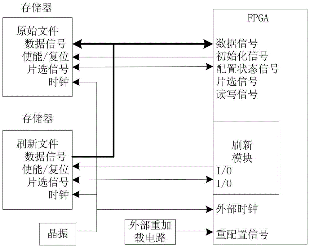
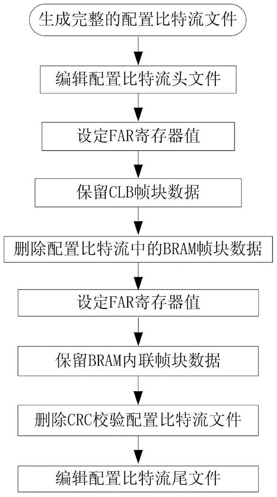
[0022] Specific implementation mode 1. Combination figure 1 with figure 2 Describe this implementation mode, SRAM type FPGA refresh circuit against single event upset; including BOOT memory and SCRUB memory. The BOOT memory stores the user function modules. After power-on, the normal loading of the FPGA is completed through the data line and the control line. After the loading is completed, the FPGA refresh module will periodically control its corresponding I / O port. The control terminal is connected, so that the configuration file in the SCRUB memory is periodically loaded into the FPGA. The file stored in the SCRUB memory is a configuration file modified from the configuration file in the BOOT memory. Before loading, the file may affect the normal operation of the FPGA. The configuration command is reset or deleted, so the FPGA keeps working normally. If a single event flip occurs in the FPGA refresh module, the FPGA can be reloaded to ensure the normal operation of the FP...
specific Embodiment approach 2
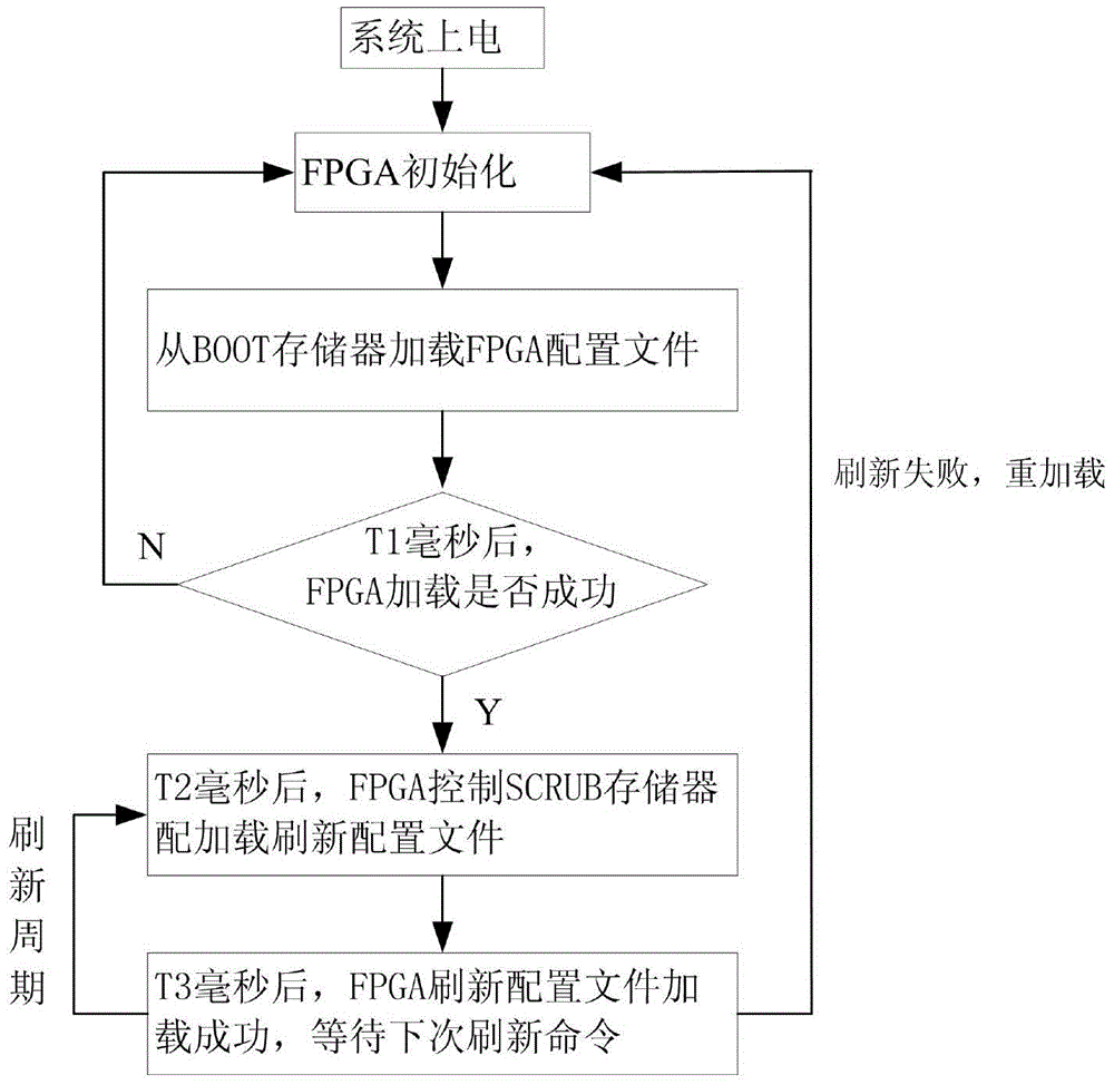
[0026] Specific embodiment two, combine image 3 Describe this embodiment mode, this embodiment mode is the refresh method of the SRAM type FPGA refresh circuit of the anti-single event reversal described in specific embodiment one, and this method is realized by the following steps:
[0027] 1. Use the programmer to burn the complete configuration file to the BOOT memory, and at the same time burn the refresh configuration file to the SCRUB memory;
[0028] 2. When the system is powered on, the FPGA clears the internal configuration data and waits for the initialization to complete;
[0029] 3. The FPGA is initialized successfully, and the BOOT memory starts to configure data, and the configuration method selects the SalveSelectMap method;
[0030] Four, T 1 Milliseconds later, the BOOT memory data configuration is completed, the enable signal is set low, the chip select signal is set high, the memory is disabled, the internal address counter is cleared, and the data output...
PUM
 Abstract
Description
Claims
Application Information
 - R&D
- Intellectual Property
- Life Sciences
- Materials
- Tech Scout
- Unparalleled Data Quality
- Higher Quality Content
- 60% Fewer Hallucinations
Browse by: Latest US Patents, China's latest patents, Technical Efficacy Thesaurus, Application Domain, Technology Topic, Popular Technical Reports.
© 2025 PatSnap. All rights reserved.Legal|Privacy policy|Modern Slavery Act Transparency Statement|Sitemap|About US| Contact US: help@patsnap.com