

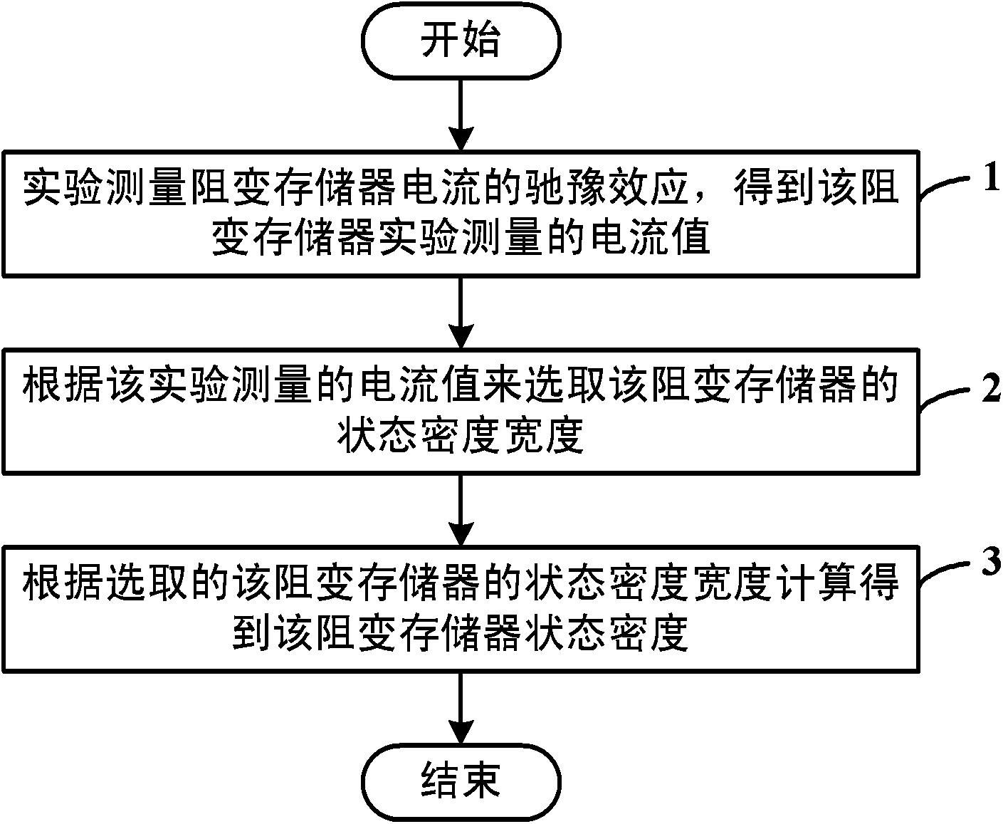
Method for measuring state density of resistive random access memory
A technology of resistive variable memory and state density, which is applied in static memory, instruments, etc., can solve the problems that the state density of resistive variable memory cannot be realized, the composition and structure of conductive filaments are uncertain, etc.
- Summary
- Abstract
- Description
- Claims
- Application Information
AI Technical Summary
Problems solved by technology
Method used
Image

Examples
Embodiment 1
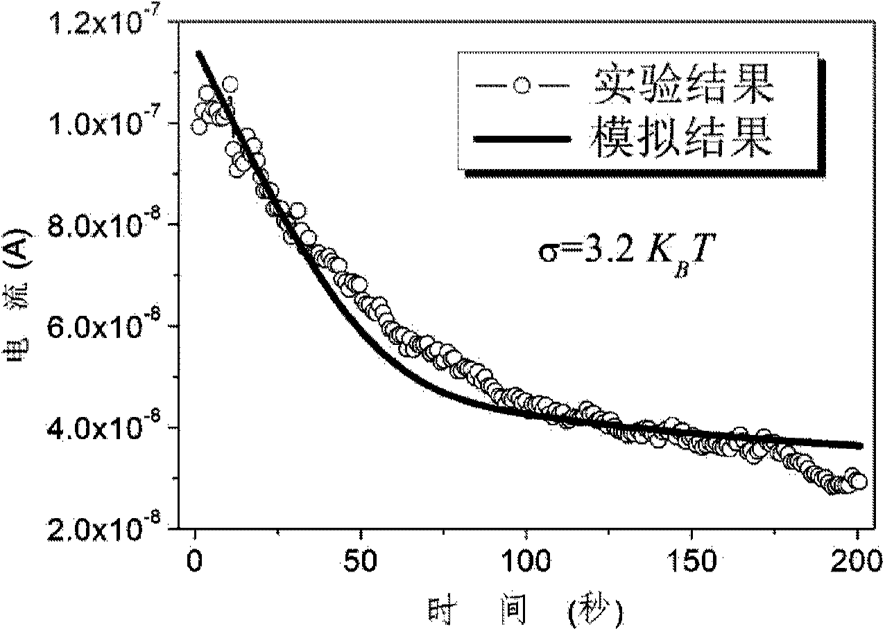
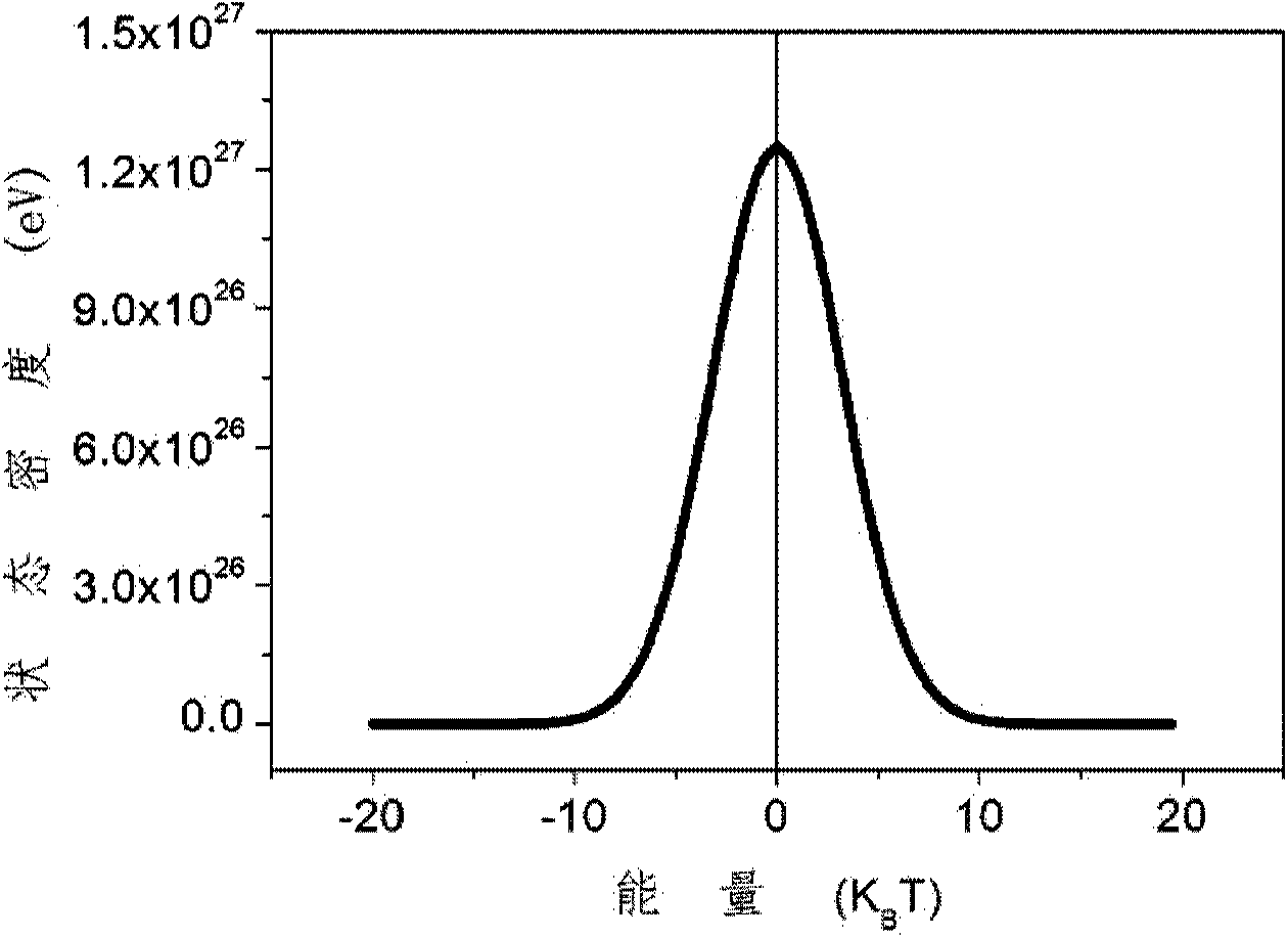
[0095] This embodiment is based on Cu / WO 3 / Pt RRAM device is implemented as an example, and the Cu / WO 3 The current value of / Pt RRAM device changes with time, the result is as follows figure 2 shown in ; then theoretically calculate Cu / WO 3 / Pt RRAM device current value changing with time, and then obtain the simulation curve consistent with the experimental results, when calculating, select the following parameters according to relevant literature reports: N t =1×10 28 m -3 , α -1= 2.7nm, v 0 =1×10 12 the s -1 , and then repeatedly select different state density widths σ and substitute into formula (1) to formula (10) to calculate Cu / WO 3 The current value of the / Pt resistive memory device changing with time, in this embodiment, when σ=3.2K B When T, the theoretical calculation results are consistent with the experimental test results, the results are as follows figure 2 shown in . Finally put σ=3.2K B Substitute T into formula (2) to get Cu / WO 3 / Pt RRAM de...
Embodiment 2
[0097] This embodiment is based on SnO 2 : F / Fe 2 o 3 / Au RRAM device is implemented as an example, and the SnO 2 : F / Fe 2 o 3 The current value of / Au resistive memory device changes with time, the results are as follows Figure 4 shown in ; then the theoretical calculation of SnO 2 : F / Fe 2 o 3 The current value of the / Au resistive memory device changes with time, and the simulation curve consistent with the experimental results is obtained. When calculating, according to the relevant literature reports, the following parameters are selected: N t =1×10 24 m -3 , α -1 = 2.7nm, v 0 =1×10 12 the s -1 , and then repeatedly select different state density widths σ and substitute into formula (1) to formula (10) to calculate SnO 2 : F / Fe 2 o 3 The current value of the / Au resistive memory device changing with time, in this embodiment, σ=2K B When T, the theoretical calculation results are consistent with the experimental test results, the results are as follows ...
PUM
 Abstract
Description
Claims
Application Information