Screen protection film and preparation method thereof
A screen protective film and protective film technology, applied in the direction of chemical instruments and methods, synthetic resin layered products, laminating devices, etc., can solve the problems of single function, anti-scratch performance, and inability to prevent the display screen from harming the eyes
- Summary
- Abstract
- Description
- Claims
- Application Information
AI Technical Summary
Problems solved by technology
Method used
Image
Examples
preparation example Construction
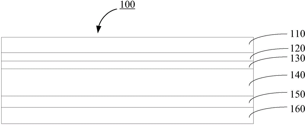
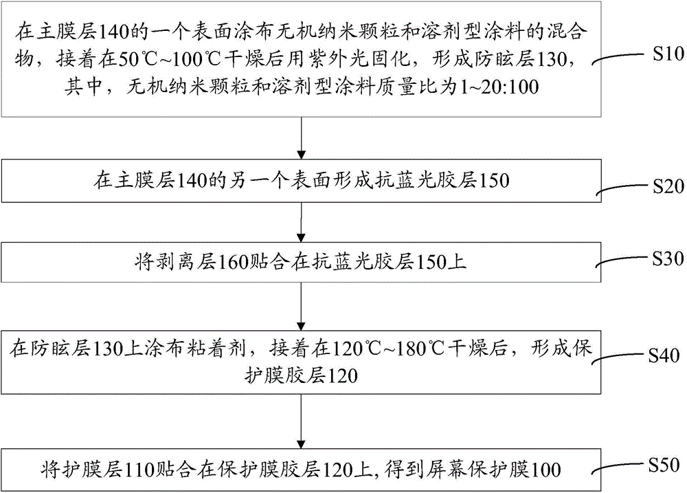
[0043] Please refer to FIG. 3 , a method for preparing a screen protective film 100 according to an embodiment includes the following steps:
[0044] S10. Coating a mixture of inorganic nanoparticles and solvent-based paint on one surface of the main film layer 140, followed by drying at 50°C to 100°C and curing with ultraviolet light to form an anti-glare layer 130, wherein the inorganic nanoparticles and solvent-based paint The coating mass ratio is 1-20:100.
[0045] The light transmittance of the main film layer 140 reaches above 80%. The haze of the main film layer 140 is less than 5%. The thickness of the main film layer 140 is uniform.
[0046] The antiglare layer 130 may have a thickness of 2 μm˜10 μm. The inorganic nanoparticles can be nano-silica or nano-alumina. It can be understood that the inorganic nanoparticles can also be other materials. The particle size of the inorganic nanoparticles may be 10 nm to 150 nm. Solvent based coatings can be urethane acryla...
Embodiment 1
[0072] A mixture of nano-silica and urethane acrylate is coated on one surface of the main film layer, wherein the mass ratio of nano-silica and urethane acrylate is 1:100, and then cured with ultraviolet light after drying at 50°C to form Anti-glare layer. The material of the main film layer is PET. The thickness of the main film layer is 50 μm. The light transmittance of the main film layer is 92%, and the haze is 1.3%. The antiglare layer formed had a thickness of 5 μm. The particle size of the nano silicon dioxide can be 10nm.
[0073] The other surface of the main film layer is coated with solvent-based acrylic and Cu by knife coating. 2+ Doped Ba 7 Si 2 o 7 Br 8 The mixture is then dried at 120°C to form an anti-blue light adhesive layer. Solventborne Acrylic and Cu 2+ Doped Ba 7 Si 2 o 7 Br 8 In the mixture, Cu 2+ Doped Ba 7 Si 2 o 7 Br 8 The mass percentage is 2%.
[0074] Attach a peeling layer with a thickness of 25 μm on the anti-blue light adhes...
Embodiment 2
[0080] A mixture of nano-alumina and epoxy acrylate is coated on one surface of the main film layer, wherein the mass ratio of nano-alumina and epoxy acrylate is 10:100, and then cured with ultraviolet light after drying at 80°C to form Anti-glare layer. The material of the main film layer is TAC. The thickness of the main film layer is 100 μm. The light transmittance of the main film layer is 91%, and the haze is 2.3%. The antiglare layer formed had a thickness of 2 μm. The particle size of the nano-alumina can be 100nm.
[0081] On the other surface of the main film layer, water-based acrylic and Zn 2+ Doped Ba 7 Si 2 o 7 Br 8 The mixture is then dried at 160°C to form an anti-blue light adhesive layer. Water-based acrylic and Zn 2+ Doped Ba 7 Si 2 o 7 Br 8 In the mixture, Zn 2+ Doped Ba 7 Si 2 o 7 Br 8 The mass percentage is 20%.
[0082] Attach a peeling layer with a thickness of 75 μm on the anti-blue light adhesive layer. The material of the peeling ...
PUM
| Property | Measurement | Unit |
|---|---|---|
| thickness | aaaaa | aaaaa |
| thickness | aaaaa | aaaaa |
| thickness | aaaaa | aaaaa |
Abstract
Description
Claims
Application Information

