

Field emission plane light source and preparing method thereof
A planar light source and field emission technology, which is applied in the field of optoelectronics, can solve problems such as the decline of emission capability, the impact on the stability and life of field emission planar light sources, and the damage of cathode electron emission materials, so as to reduce the area, alleviate the area effect, reduce The effect of the number of positive ions
- Summary
- Abstract
- Description
- Claims
- Application Information
AI Technical Summary
Problems solved by technology
Method used
Image

Examples
Embodiment Construction
[0035] The following descriptions are preferred implementations of the embodiments of the present invention. It should be pointed out that those skilled in the art can make some improvements and modifications without departing from the principles of the embodiments of the present invention. These improvements And retouching are also regarded as the scope of protection of the embodiments of the present invention.
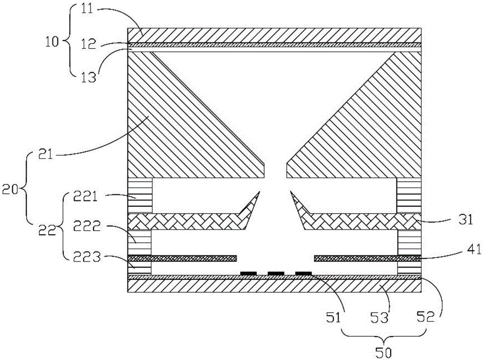
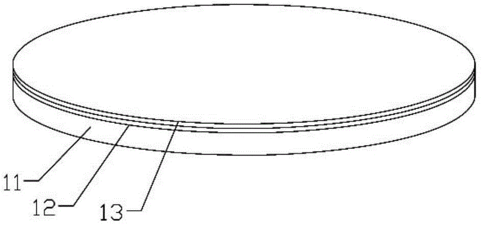
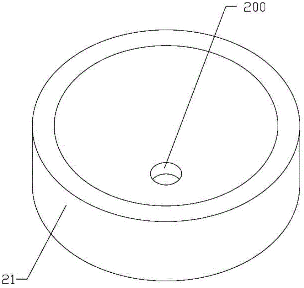
[0036] figure 1 is a cross-sectional view of a field emitting planar light source according to an embodiment of the present invention; figure 2 It is an anode structure diagram of a field emission planar light source according to an embodiment of the present invention; image 3 It is a structure diagram of the isolated main body of the field emission planar light source according to the embodiment of the present invention; Figure 4 It is the structure diagram of the focusing pole of the field emission planar light source in the embodiment of the present invention...
PUM
 Abstract
Description
Claims
Application Information