Formation method of semiconductor device

A semiconductor and device technology, applied in the field of semiconductor device formation, can solve problems such as poor performance of transistors, achieve the effects of enhancing reliability and stability, adjusting threshold voltage, and improving performance

Inactive Publication Date: 2014-09-24
SEMICON MFG INT (SHANGHAI) CORP
View PDF5 Cites 2 Cited by
  • Summary
  • Abstract
  • Description
  • Claims
  • Application Information

AI Technical Summary

Problems solved by technology

[0009] The problem solved by the present invention is that the metal gate formed by using the prior art is applied to the transistor, resulting in poor performance of the transistor

Method used


Image

  • Formation method of semiconductor device
  • Formation method of semiconductor device
  • Formation method of semiconductor device

Examples


Embodiment Construction

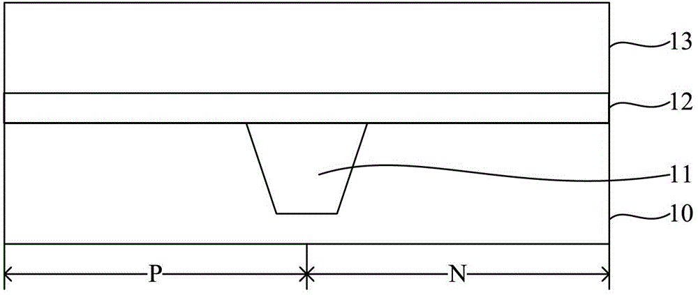
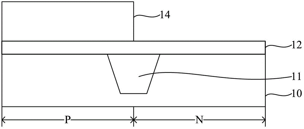
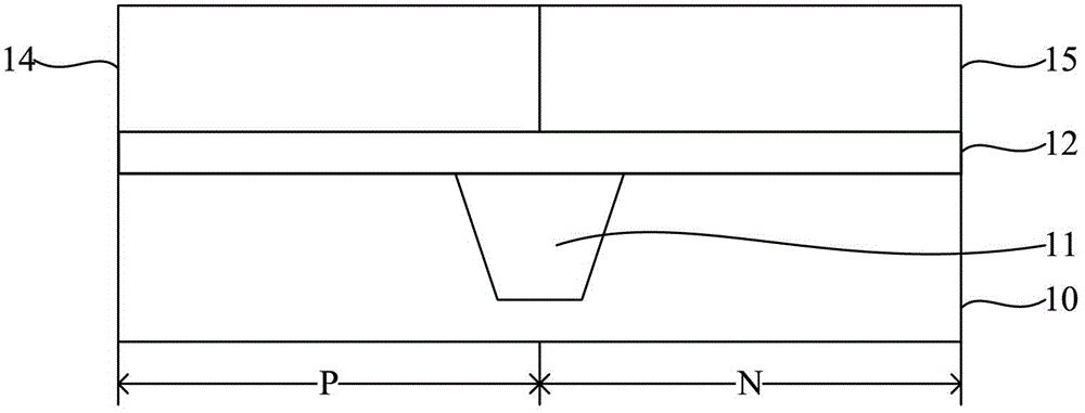
[0049] The inventor has conducted research on the problems existing in the prior art and found that: with reference to figure 2 and image 3 , when etching to remove the TiAlN layer in the N-type active region, it will damage the HfO by over-etching 2 Layer 12. Damaged HfO 2 As the layer becomes thinner, the TiN in the subsequent process of forming the TiN layer 15 of the N-type active region may diffuse into the substrate 10, which will affect the reliability and stability of the NMOS transistor. Moreover, HfO 2 As the thickness of the gate dielectric layer decreases, the gate leakage current will increase, resulting in poor performance of the transistor.

[0050]The inventor obtained a new method for forming a semiconductor device through creative research. In order to make the above objects, features and advantages of the present invention more comprehensible, specific implementations of the present invention will be described in detail below in conjunction with the a...


PUM


Abstract

Disclosed is a formation method of a semiconductor device. The method comprises: providing a semiconductor substrate, and forming an isolation structure in the substrate, wherein the isolation structure isolates the substrate to a first active area and a second active area, and the types of the first active area and the second active area are opposite; forming a high-k dielectric layer and a conducting layer on the high-k dielectric layer on the substrate, defining the conducting layer disposed in the first active area as a first conducting layer, and defining the conducting layer disposed on the second active area as a second conducting layer; carrying out work function adjustment on the first conducting layer and/or the second conducting layer; and after the work function adjustment is carried out, patterning the first conducting layer, the second conducting layer and the high-k dielectric layer, and forming a first grid electrode disposed in the first active area, a first high-k dielectric layer disposed below the first grid electrode, a second grid electrode disposed in the second active area and a second high-k dielectric layer disposed below the second grid electrode. According to the invention, the work function adjustment is carried out on the first conducting layer and/or the second conducting layer, an etching process is unnecessary, and the high-k dielectric layer is not damaged.

Description

technical field [0001] The invention relates to the technical field of semiconductors, in particular to a method for forming a semiconductor device. Background technique [0002] In the existing metal gate technology, the threshold voltage of the transistor can be adjusted by adjusting the work function of the transistor, thereby improving the performance of the transistor. Considering that the working principles of NMOS transistors and PMOS transistors are different, if the work function of the metal gate of the NMOS transistor is reduced and the work function of the metal gate of the PMOS transistor is increased, the threshold voltage of the NMOS transistor and the PMOS transistor can be reduced, thereby improving the performance of the transistor. For example, the work function range of the metal gate of the NMOS transistor is about 4.1-4.3 eV, and the work function range of the metal gate of the PMOS transistor is about 5.0-5.2 eV. Therefore, in the prior art, different...

Claims


Application Information

Patent Timeline
Patent Type & Authority Applications(China)
IPC IPC(8): H01L21/28H01L21/8238
CPCH01L21/28008H01L21/8238
Inventor 何永根陈勇
Owner SEMICON MFG INT (SHANGHAI) CORP
Why Eureka
Try Eureka