Organic electroluminescent device
An electroluminescent device and luminescence technology, which is applied in the direction of organic semiconductor devices, electric solid devices, organic semiconductor device materials, etc., can solve the problems of short service life and achieve long service life and reduce the effect of water and oxygen penetration
- Summary
- Abstract
- Description
- Claims
- Application Information
AI Technical Summary
Problems solved by technology
Method used
Image
Examples
Embodiment 1
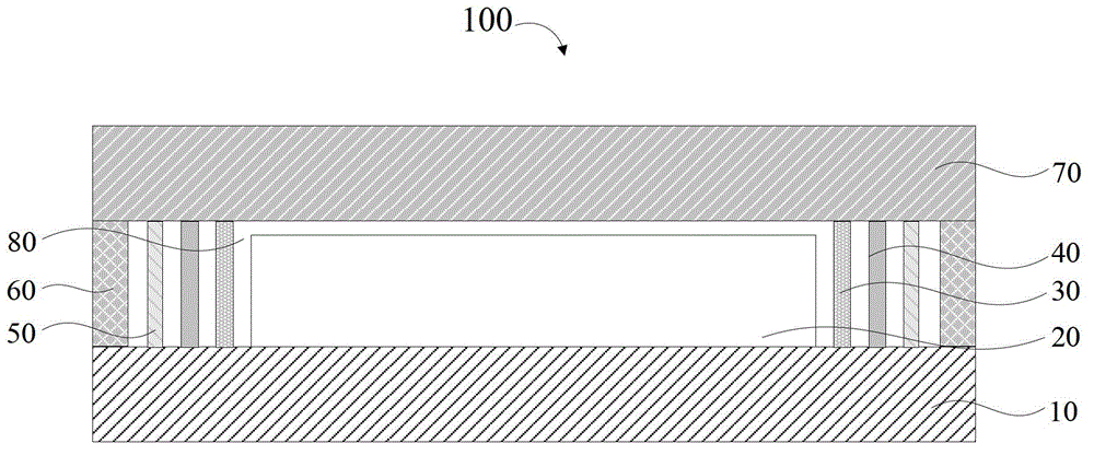
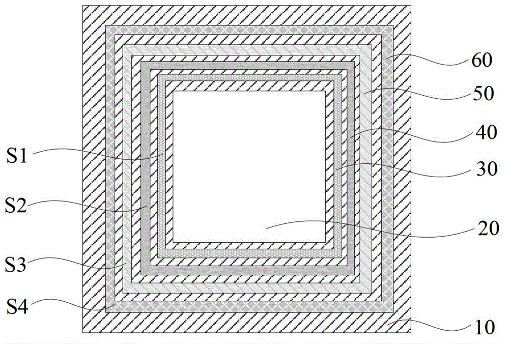
[0066] After the glass substrate is cleaned and dried, an anode, a hole transport layer, a light-emitting layer, an electron injection layer and a cathode are sequentially formed on the glass substrate by vacuum evaporation, and an anode, a hole transport layer, a light-emitting layer, an electron injection layer and a cathode The organic light-emitting unit stacked on the glass substrate is sequentially stacked, and the organic light-emitting unit is arranged in the middle of the glass substrate and covers part of the surface of the glass substrate; wherein, the anode is formed of indium tin oxide, and the thickness of the anode is 100 nanometers; the hole The transport layer is formed of N,N'-diphenyl-N,N'-di(1-naphthyl)-1,1'-biphenyl-4,4'-diamine, and the thickness of the hole transport layer is 50 nanometer; the light-emitting layer is formed by (8-hydroxyquinoline)-aluminum, and the thickness of the light-emitting layer is 30 nanometers; the electron injection layer is for...
Embodiment 2
[0074] After the glass substrate is cleaned and dried, an anode, a hole transport layer, a light-emitting layer, an electron injection layer and a cathode are sequentially formed on the glass substrate by vacuum evaporation, and an anode, a hole transport layer, a light-emitting layer, an electron injection layer and a cathode The organic light-emitting unit stacked on the glass substrate is sequentially stacked, and the organic light-emitting unit is arranged in the middle of the glass substrate and covers part of the surface of the glass substrate; wherein, the anode is formed of indium tin oxide, and the thickness of the anode is 100 nanometers; the hole The transport layer is formed of N,N'-diphenyl-N,N'-di(1-naphthyl)-1,1'-biphenyl-4,4'-diamine, and the thickness of the hole transport layer is 50 nanometer; the light-emitting layer is formed by (8-hydroxyquinoline)-aluminum, and the thickness of the light-emitting layer is 30 nanometers; the electron injection layer is for...
Embodiment 3
[0082] After the glass substrate is cleaned and dried, an anode, a hole transport layer, a light-emitting layer, an electron injection layer and a cathode are sequentially formed on the glass substrate by vacuum evaporation, and an anode, a hole transport layer, a light-emitting layer, an electron injection layer and a cathode The organic light-emitting unit stacked on the glass substrate is sequentially stacked, and the organic light-emitting unit is arranged in the middle of the glass substrate and covers part of the surface of the glass substrate; wherein, the anode is formed of indium tin oxide, and the thickness of the anode is 100 nanometers; the hole The transport layer is formed of N,N'-diphenyl-N,N'-di(1-naphthyl)-1,1'-biphenyl-4,4'-diamine, and the thickness of the hole transport layer is 50 nanometer; the light-emitting layer is formed by (8-hydroxyquinoline)-aluminum, and the thickness of the light-emitting layer is 30 nanometers; the electron injection layer is for...
PUM
 Abstract
Description
Claims
Application Information


