Detection method for under-etching of through holes

A technology of through-hole etching and detection methods, which is applied in semiconductor/solid-state device testing/measurement, electrical components, circuits, etc., can solve problems such as difficult online process window optimization and provide effective reference, and achieve semiconductor online manufacturing and yield Improve security, improve monitoring sensitivity, and improve the effect of crawling rate

Active Publication Date: 2014-10-01
SHANGHAI HUALI MICROELECTRONICS CORP
View PDF5 Cites 5 Cited by
  • Summary
  • Abstract
  • Description
  • Claims
  • Application Information

AI Technical Summary

Problems solved by technology

[0004] Therefore, the above two detection methods for insufficient via etching have great shortcomings, and it is difficult to provide an effective reference for the optimization of the online process window

Method used


Image

  • Detection method for under-etching of through holes
  • Detection method for under-etching of through holes
  • Detection method for under-etching of through holes

Examples


Embodiment 1

[0039] figure 1 A schematic flow chart of the method for detecting insufficient etching of via holes provided in this embodiment. Such as figure 1 As shown, the detection method includes steps:

[0040] Step S1: Build a plurality of test modules on the semiconductor substrate, each test module simulates the SRAM device structure, wherein each transistor of the test module is an NMOS device in a P well, and the active region of the simulated transmission gate transistor is not formed grid.

[0041] Specifically, since each test module simulates a SRAM device structure, each test module includes two analog pass-gate transistors, two pull-up transistors and two pull-down transistors. Unlike the SRAM device structure, the test modules These transistors are all NMOS devices in the P-well. In addition, another difference of the present invention is that the analog pass-gate transistor only has an active area without forming a gate on the active area.

[0042] The formation meth...

Embodiment 2

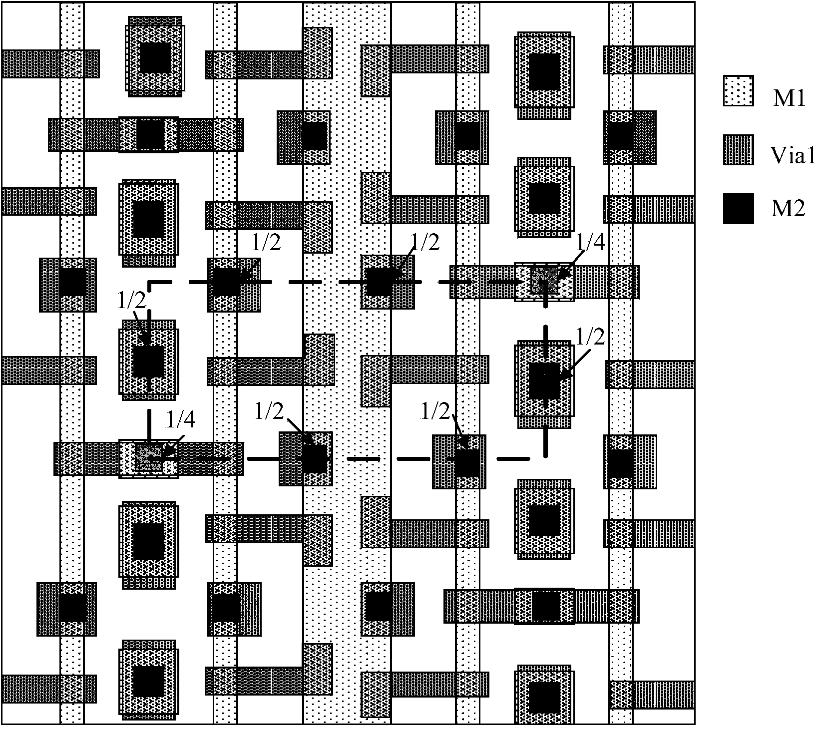
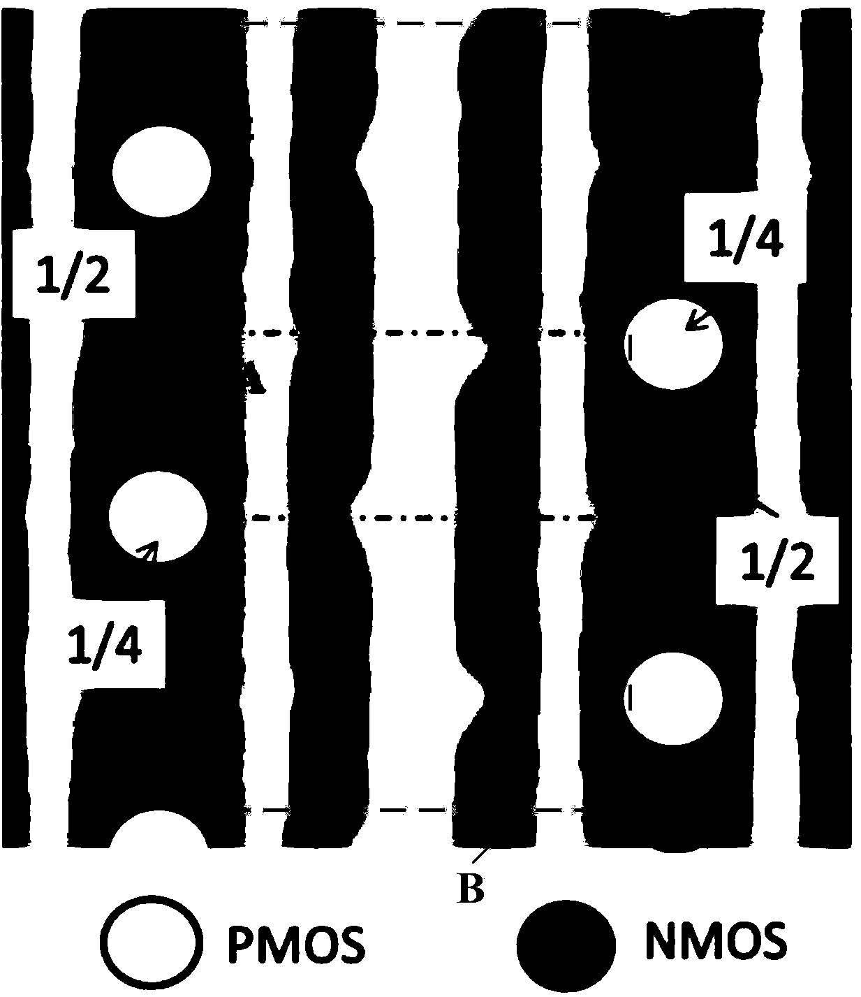
[0053] Although the above-mentioned embodiment can increase the detection via hole ( Figure 2b In the case of etching at A), but for multiple vias connected by the same metal interconnection line, such as Figure 2b In the B area, if some of the through holes are under-etched, it will still not be detected. Therefore, in order to further increase the number of detectable vias, this embodiment improves the method for forming vias and metal interconnection lines.

[0054] Please refer to Figure 5a to Figure 5g , which is a schematic diagram of each step of the method for forming conductive vias and metal interconnections in this embodiment. In this embodiment, the steps of establishing test modules, forming a plurality of contact holes on each test module and filling metal are the same as those in the first embodiment, and will not be repeated here.

[0055] Please refer to Figure 5a and Figure 5b After the contact hole is formed, filled with metal and planarized, a die...


PUM


Abstract

The invention discloses a detection method for under-etching of through holes. The method comprises the following steps: a plurality of test modules are built on the substrate of a semiconductor, each test module simulates an SRAM device structure and comprises two simulation transmission gate transistors, two simulation pull-up transistors and two simulation pull-down transistors; the simulation transmission gate transistors, the simulation pull-up transistors and the simulation pull-down transistors are NMOS devices in a P trap, and a grid electrode is not formed in the active area of each simulation transmission gate transistor; a plurality of contact holes filled with metal are formed in each test module; the contact holes are connected with the position, corresponding to the grid electrode, of the active area of each simulation transmission gate transistor at least; metal interconnecting wires and conductive through holes are formed in the contact holes; test modules are scanned under the positive potential condition by an electron beam defect scanner, and the defect of under-etching of through holes of the test modules is detected according to image characteristic patterns obtained through scanning. The method provided by the invention can increase the capturing rate of the defect of under-etching.

Description

technical field [0001] The invention relates to semiconductor manufacturing technology, in particular to a method for detecting insufficient etching of through holes. Background technique [0002] With the development of integrated circuit technology and the scaling down of critical dimensions, the etching of copper connection vias in the back-end process of semiconductor devices is insufficient (such as figure 1 Shown) and via missing defects are increasingly becoming one of the bottlenecks hindering the development of integrated circuits. For example, in the etching process of first etching the hard mask (Hard Mask Etch) and then etching the through hole (All in One Etch), the under-etching defects are often affected by the cleaning process after the hard mask etching, the via etching itself and the via etching. The common influence of the photolithography process, when some of the process windows are not optimized enough, defects will appear, which becomes a major killer...

Claims


Application Information

Patent Timeline
Patent Type & Authority Applications(China)
IPC IPC(8): H01L21/66
CPCH01L22/12H01L22/26
Inventor 范荣伟陈宏璘龙吟顾晓芳
Owner SHANGHAI HUALI MICROELECTRONICS CORP
Why Eureka
Try Eureka