Supercharge Your Innovation With Domain-Expert AI Agents!

Organic light-emitting diode and preparation method thereof

An electroluminescent device and luminescent technology, applied in the direction of organic semiconductor devices, organic semiconductor device materials, electric solid devices, etc., can solve the problems of material aging, failure, and short life of light-emitting devices, and achieve long life and water resistance. Oxygen corrosion, improve the effect of waterproof oxygen ability

Inactive Publication Date: 2014-10-01
OCEANS KING LIGHTING SCI&TECH CO LTD +2
View PDF10 Cites 0 Cited by
  • Summary
  • Abstract
  • Description
  • Claims
  • Application Information

AI Technical Summary

Problems solved by technology

[0003] After the organic electroluminescent device is corroded by moisture and moisture, the material of the internal components of the organic electroluminescent device will be aged and then become invalid, so that the life of the organic electroluminescent device is relatively short

Method used


Image

  • Organic light-emitting diode and preparation method thereof
  • Organic light-emitting diode and preparation method thereof
  • Organic light-emitting diode and preparation method thereof

Examples


preparation example Construction

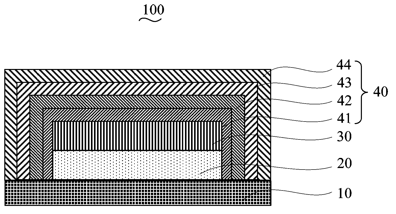
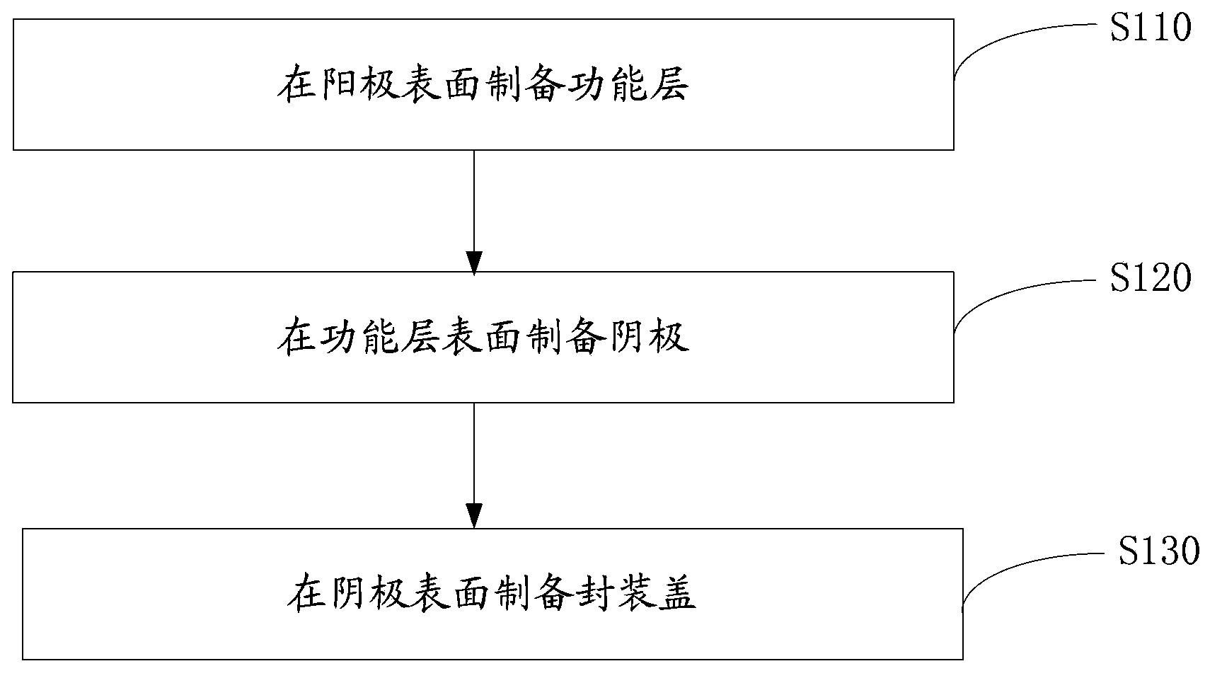
[0047] see also figure 2 , the preparation method of the organic electroluminescent device 100 of one embodiment, it comprises the following steps:

[0048] Step S110 , forming a functional layer 20 on the anode 10 .

[0049] The functional layer 20 includes a hole injection layer, a hole transport layer, a light emitting layer, an electron transport layer, and an electron injection layer stacked in this order.

[0050] The anode 10 may be a conductive glass substrate or a conductive organic polyethylene terephthalate (PET) film substrate. The anode 10 has an ITO layer prepared with an anode pattern. The thickness of the ITO layer is 100 nm to 150 nm.

[0051] Before forming the functional layer 20 , the surface of the anode 10 is pretreated to remove contaminants on the surface of the substrate 10 , and surface activation is performed to increase the oxygen content on the surface of the anode 10 to improve the work function of the surface of the anode 10 . Specifically, ...
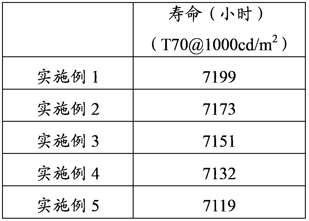
Embodiment 1

[0082] The structure prepared in this example is: ITO / NPB:MoO 3 / TCTA / TPBI:Ir(ppy) 3 / Bphen / Bphen:CsN 3 / Al / organic electroluminescent device with encapsulation cover; wherein, the slanted bar " / " indicates the layered structure, and the colon ":" indicates doping, the same below.

[0083] The preparation method of the above-mentioned organic electroluminescent device comprises the following steps:

[0084] 1. Form a functional layer on the anode.

[0085] The anode 10 is conductive glass. The anode 10 has an ITO layer prepared with an anode pattern. The thickness of the ITO layer was 150 nm.

[0086] Before forming the functional layer 20 , the surface of the anode 10 is pretreated to remove contaminants on the surface of the substrate 10 , and surface activation is performed to increase the oxygen content on the surface of the anode 10 to improve the work function of the surface of the anode 10 . Specifically, the anode 10 was successively cleaned by ultrasonic waves ...

Embodiment 2

[0103] The structure prepared in this example is: ITO / NPB:MoO 3 / TCTA / TPBI:Ir(ppy) 3 / Bphen / Bphen:CsN 3 / Al / organic electroluminescent device with encapsulation lid.

[0104] The preparation method of the above-mentioned organic electroluminescent device comprises the following steps:

[0105] 1. Form a functional layer on the anode.

[0106] The anode 10 is conductive glass. The anode 10 has an ITO layer prepared with an anode pattern. The thickness of the ITO layer was 120 nm.

[0107] Before forming the functional layer 20 , the surface of the anode 10 is pretreated to remove contaminants on the surface of the substrate 10 , and surface activation is performed to increase the oxygen content on the surface of the anode 10 to improve the work function of the surface of the anode 10 . Specifically, the anode 10 was successively cleaned by ultrasonic waves for 5 min to remove acetone, ethanol, ionized water and ethanol, and then dried with nitrogen and oven dried.

[01...


PUM

PropertyMeasurementUnit
Thicknessaaaaaaaaaa
Thicknessaaaaaaaaaa
Thicknessaaaaaaaaaa

Abstract

An organic light-emitting diode comprises a positive pole, a light-emitting layer, a negative pole and a packaging cover which are stacked in sequence. The light-emitting layer and the negative pole are packaged on the positive pole through the packaging cover, and the packaging cover comprises a first organic barrier layer, a first inorganic barrier layer formed on the surface of the first organic barrier layer, a second organic barrier layer formed on the surface of the first inorganic barrier layer and a second inorganic barrier layer formed on the surface of the second organic barrier layer. Materials of the first organic barrier layer comprise a hole transport material and an electron transport material; materials of the first inorganic barrier layer comprise a nitride, a boride and a selenide; materials of the second organic barrier layer comprise a hole transport material and an electron transport material; and materials of the second inorganic barrier layer comprise a nitride and a selenide. The organic light-emitting diode is long in service life. The invention further provides a preparation method for preparing the organic light-emitting diode.

Description

technical field [0001] The present invention relates to an organic electroluminescence device and a preparation method thereof. Background technique [0002] An organic electroluminescent device (OLED) is a current-mode semiconductor light-emitting device based on organic materials. Its typical structure is to prepare a layer of organic light-emitting material with a thickness of tens of nanometers on ITO glass as a light-emitting layer, and a layer of metal electrode with low work function is placed above the light-emitting layer. When a voltage is applied to the electrodes, the light-emitting layer produces light radiation. [0003] After the organic electroluminescent device is corroded by moisture and moisture, the materials of the internal elements of the organic electroluminescent device will be aged and then fail, so that the lifespan of the organic electroluminescent device is short. SUMMARY OF THE INVENTION [0004] Based on this, it is necessary to provide an o...

Claims


Application Information

Patent Timeline
IPC IPC(8): H01L51/50H01L51/52H01L51/54H01L51/56
CPCH10K50/8445H10K50/841H10K2102/00H10K71/00
Inventor 周明杰钟铁涛王平冯小明
Owner OCEANS KING LIGHTING SCI&TECH CO LTD
Features
  • R&D
  • Intellectual Property
  • Life Sciences
  • Materials
  • Tech Scout
  • Unparalleled Data Quality
  • Higher Quality Content
  • 60% Fewer Hallucinations
Learn More