A method for detecting insufficient etching of through holes
A technology for through-hole etching and detection methods, which is applied in semiconductor/solid-state device testing/measurement, electrical components, semiconductor/solid-state device manufacturing, etc. The effects of manufacturing and yield improvement guarantee, improvement of capture rate, and improvement of monitoring sensitivity
- Summary
- Abstract
- Description
- Claims
- Application Information
AI Technical Summary
Problems solved by technology
Method used
Image
Examples
Embodiment 1
[0039] image 3 A schematic flowchart of a method for detecting insufficient etching of via holes provided in this embodiment. Such as image 3 As shown, the detection method includes steps:
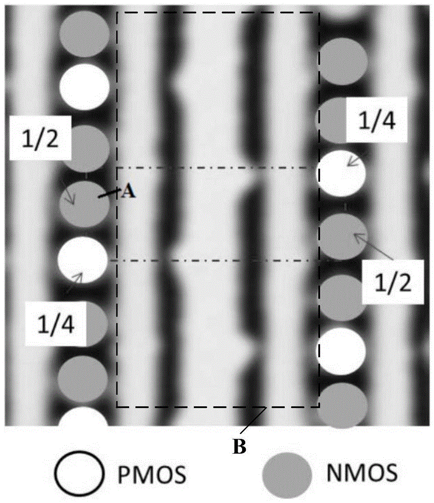
[0040] Step S1: Build a plurality of test modules on the semiconductor substrate, each test module simulates the SRAM device structure, wherein the transistors in the test module are all PMOS devices in the N well and no gate is formed on the active region of the simulated transmission gate transistor pole.
[0041] Specifically, since each test module simulates a SRAM device structure, each test module includes 2 analog pass-gate transistors, two pull-up transistors and two pull-down transistors. Unlike the SRAM device structure, the These transistors are all PMOS devices in N-well. In addition, another difference of the present invention is that the analog pass-gate transistor only has an active area without forming a gate on the active area.
[0042] The formation method of this ...
Embodiment 2
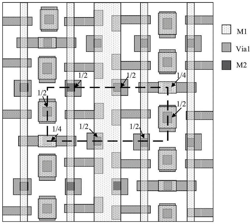
[0053] Although the above-mentioned embodiment can increase the detection via hole ( Figure 2b In the case of etching at A), but for multiple vias connected by the same metal interconnection line, such as Figure 2b In the B area, if some of the through holes are under-etched, it will still not be detected. Therefore, in order to further increase the number of detectable vias, this embodiment improves the method for forming vias and metal interconnection lines.
[0054] Please refer to Figure 5a to Figure 5g , which is a schematic diagram of each step of the method for forming conductive vias and metal interconnections in this embodiment. In this embodiment, the steps of establishing test modules, forming a plurality of contact holes on each test module and filling metal are the same as those in the first embodiment, and will not be repeated here.
[0055] Please refer to Figure 5a and Figure 5b After the contact hole is formed, filled with metal and planarized, a die...
PUM
 Abstract
Description
Claims
Application Information


