A single-mode silicon-based hybrid laser light source with silicon waveguide output

A technology of laser light source and silicon waveguide, which is applied in the direction of semiconductor lasers, optical waveguide semiconductor structures, lasers, etc., can solve problems such as limiting the development of single-mode silicon-based hybrid semiconductor lasers, reducing laser mode gain, and increasing threshold current density. Facilitate large-scale production, achieve single longitudinal mode output, and reduce the effect of threshold current density

Active Publication Date: 2017-10-03
INST OF SEMICONDUCTORS - CHINESE ACAD OF SCI
View PDF4 Cites 0 Cited by
  • Summary
  • Abstract
  • Description
  • Claims
  • Application Information

AI Technical Summary

Problems solved by technology

However, the reduction of the confinement factor will reduce the modal gain of the laser, which will lead to an increase in the threshold current density; and if the silicon waveguide on SOI is too thick (higher than 400nm), it will cause the laser to output multiple transverse modes, which is not conducive to CMOS. Integration of lasers with other single-mode devices (such as amplifiers, modulators, etc.) on a compatible silicon-based platform
These factors limit the development of single-mode silicon-based hybrid semiconductor lasers

Method used


Image

  • A single-mode silicon-based hybrid laser light source with silicon waveguide output
  • A single-mode silicon-based hybrid laser light source with silicon waveguide output
  • A single-mode silicon-based hybrid laser light source with silicon waveguide output

Examples


Embodiment

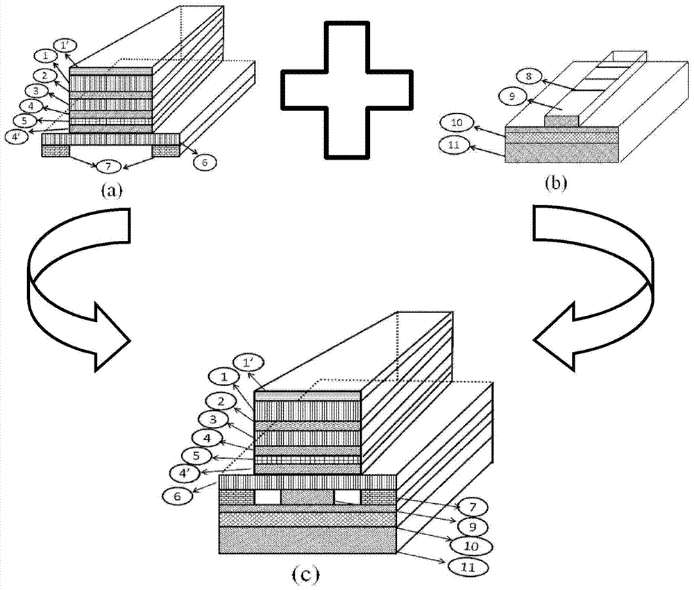
[0040] figure 1 (a) to figure 1 (c) is a schematic diagram of the evolution of the three-dimensional structure of a single-mode silicon-based hybrid laser light source output by a silicon waveguide according to an embodiment of the present invention. figure 1 (a) is a III-V taper gain structure, where the length of the taper is 500 μm and the width of the top is 0.4 μm; figure 1 (b) is an SOI ridge waveguide structure, in which the height of the silicon on the top layer of SOI is 0.34 μm, and the etching depth of the silicon waveguide and the periodic microgrooves are both 0.2 μm; figure 1 (c) is a single-mode silicon-based hybrid laser light source obtained after reflow soldering. The reflow soldering metal is an AuSn alloy, which forms an ohmic contact after annealing and is used as the negative electrode of the device; the lasing wavelength of the single-mode silicon-based hybrid laser source is 1490nm. The total device length is 1000 μm.

[0041] figure 2 (a) is a sch...


PUM


Abstract

The invention discloses a single-mode silicon-based hybrid laser light source output by a silicon waveguide. The laser light source includes a stacked tapered (Taper) gain structure and an SOI ridge waveguide structure, wherein the tapered gain structure is passed through reflow soldering technology. flip-chip bonding on the SOI ridge waveguide structure. The invention improves the confinement factor of the active region by introducing the III-V family Taper structure and growing the optical lower confinement layer in the periodic microgroove hybrid laser, thereby increasing the mode gain in the III-V family; at the same time, the introduction of the Taper structure The efficient coupling between the III‑V group structure and the silicon waveguide is guaranteed, and the single longitudinal mode laser is output from the silicon waveguide. The invention has low manufacturing cost, can be used for silicon-based optical interconnection, and laser light source in optical communication, improves the coupling efficiency of III-V light source and silicon waveguide, and realizes an efficient coupling single-mode hybrid silicon-based semiconductor laser light source.

Description

technical field [0001] The invention relates to a laser light source in the field of silicon-based platform optoelectronic integration, in particular to a single-mode silicon-based hybrid laser light source output by a silicon waveguide in silicon-based hybrid integration. Background technique [0002] With the development of optical communication technology and microelectronics technology, people require faster and faster computing speed of computers and smaller and smaller device sizes. However, the interconnection delay effect and energy consumption of integrated circuits based on electrical interconnection limit the further development of microelectronics technology. Compared with traditional electrical interconnection technology, optical interconnection technology using optical waves as information carriers , has the advantages of no signal interference, fast response, low power consumption, and large bandwidth. Therefore, one of the current research hotspots is to rea...

Claims


Application Information

Patent Timeline
Patent Type & Authority Patents(China)
IPC IPC(8): H01S5/22H01S5/343
Inventor 郑婉华王海玲冯朋张斯日古楞王宇飞刘安金
Owner INST OF SEMICONDUCTORS - CHINESE ACAD OF SCI
Why Eureka
Try Eureka