Array substrate and driving method thereof, as well as display device
A technology of array substrate and display switch, applied in static indicators, instruments, etc., can solve the problems of rising power consumption of storage capacitors, large output voltage swing of data voltage signal, and large voltage fluctuation range, etc., to reduce power consumption, The effect of reducing swing
- Summary
- Abstract
- Description
- Claims
- Application Information
AI Technical Summary
Problems solved by technology
Method used
Image
Examples
Embodiment 1
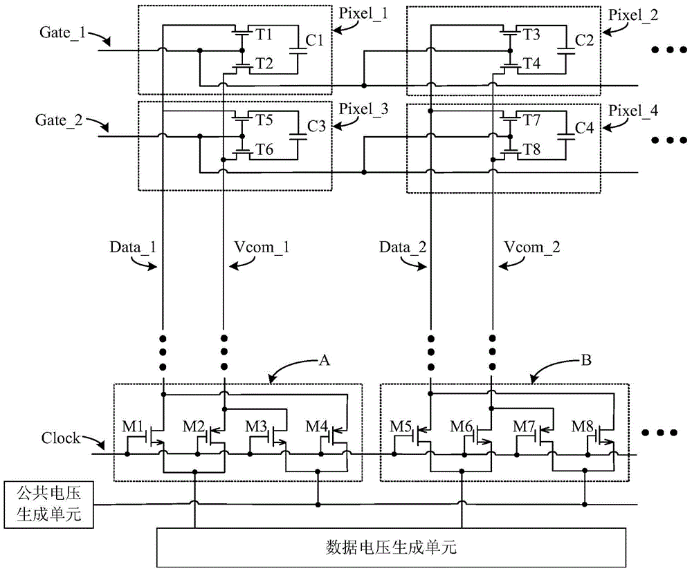
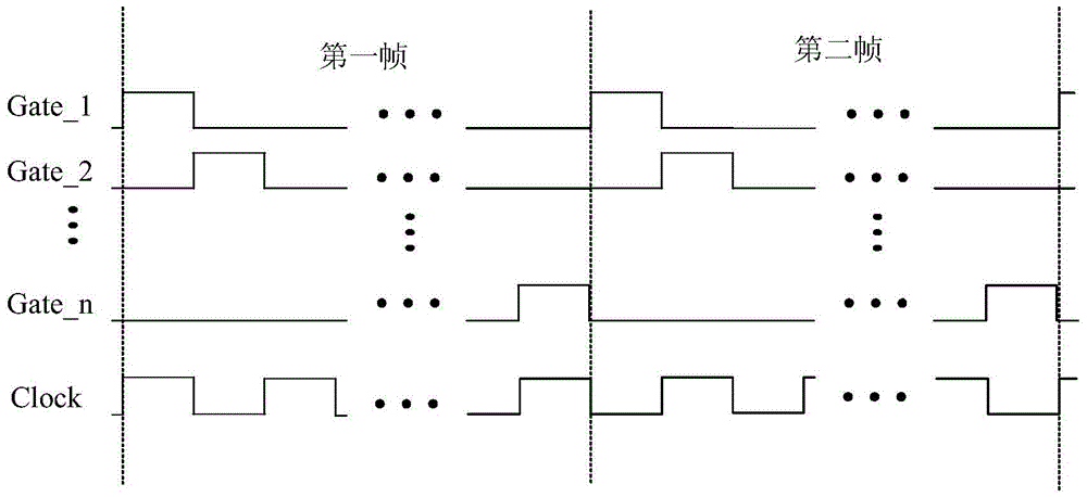
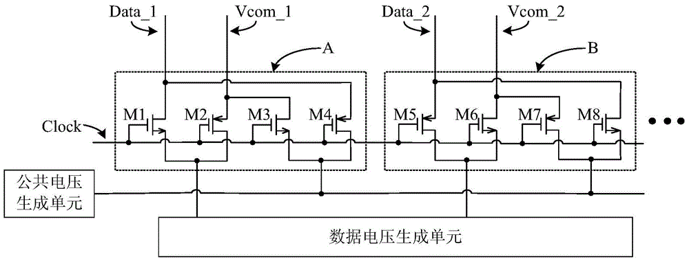
[0052] figure 1 is a schematic diagram of the array substrate provided in Embodiment 1 of the present invention, figure 2 for figure 1 The timing diagram of the array substrate shown, image 3 for figure 1 A schematic diagram of the switch control unit in the Figure 1 to Figure 3 As shown, the array substrate includes: a common voltage generating unit, a data voltage generating unit, a timing control unit, several gate lines, data lines and common voltage lines, the gate lines and data lines define several pixel units, and the pixel units include: The first display switch tube and the storage capacitor, the control pole of the first display switch tube is connected to the gate line of the corresponding row, the first pole of the first display switch tube is connected to the data line of the corresponding column, and the second pole of the display switch tube is connected to the corresponding column. The first end of the storage capacitor is connected, and the second end ...
Embodiment 2
[0087] Figure 5 is a schematic diagram of the array substrate provided in Embodiment 2 of the present invention, Image 6 for Figure 5 The timing diagram of the array substrate shown, Figure 7 for Figure 5 A schematic diagram of the switch control unit in the Figure 5 to Figure 7 as shown, Figure 5 The array substrate shown with the figure 1 The difference between the array substrates shown is that Figure 7 The timing control unit in the array substrate shown includes two timing control lines Clock_1 (Clock_2), the first control switch M1 and the third control switch M3 in the switch control unit A are connected to the timing control line Clock_1, and the switch control unit A The second control switch tube M2 and the fourth control switch tube M4 in the switch control unit B are connected to the timing control line Clock_2; the first control switch tube M5 and the third control switch tube M7 in the switch control unit B are connected to the timing control line C...
Embodiment 3
[0111] Embodiment 3 of the present invention provides a display device. The display device includes an array substrate, wherein the array substrate can be the array substrate provided in Embodiment 1 or Embodiment 2 above. For details, please refer to Embodiment 1 or Embodiment 2 above. The description in II will not be repeated here.
[0112] Embodiment 3 of the present invention provides a display device, which includes: an array substrate, and the array substrate includes: a common voltage generation unit, a timing control unit, several data voltage generation units, a switch control unit, and a pixel unit, wherein the switch The control unit is connected with the common voltage generation unit, the timing control unit, the data voltage generation unit, the common voltage line and the data line, and the switch control unit is used to switch the voltage signal loaded on the data line and the common voltage line, thereby realizing the display device In order to meet the polar...
PUM
 Abstract
Description
Claims
Application Information


