Circuit board with high-density circuits and method for manufacturing the circuit board

A manufacturing method and high-density technology, applied in the directions of printed circuit components, electrical connection printed components, and electrical connection formation of printed components, can solve the problems of electrical failure of conductive holes, gaps cannot be filled, etc., and achieve stable electrical performance. Effect

Inactive Publication Date: 2014-10-15
QI DING TECHNOLOGY QINHUANGDAO CO LTD +1
View PDF2 Cites 5 Cited by
  • Summary
  • Abstract
  • Description
  • Claims
  • Application Information

AI Technical Summary

Problems solved by technology

Since both ends of the via hole are closed, the void cannot be filled, resulting in electrical failure of the formed conductive hole

Method used


Image

  • Circuit board with high-density circuits and method for manufacturing the circuit board
  • Circuit board with high-density circuits and method for manufacturing the circuit board
  • Circuit board with high-density circuits and method for manufacturing the circuit board

Examples


Embodiment Construction

[0021] Hereinafter, the technical solution provides the circuit board with the high-density circuit and its manufacturing method with specific examples.

[0022] The manufacturing method of the circuit board of the high-density circuit provided by the embodiment of the technical solution comprises the following steps:

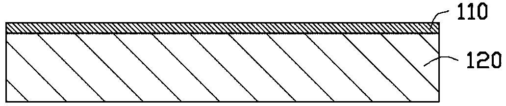
[0023] For a first step, see figure 1 , providing a first copper foil 110 .

[0024] The first copper foil 110 is a copper foil with a thickness of 5 microns to 15 microns.

[0025] In this embodiment, the first copper foil 110 is supported in order to facilitate the subsequent manufacturing process. A support plate 120 can also be detachably attached to one side surface of the first copper foil 110 . The support plate 120 can be made of metal or non-metal. The thickness of the support plate 120 is not limited, it only needs to have a flat surface and be able to support the first copper foil 110 .

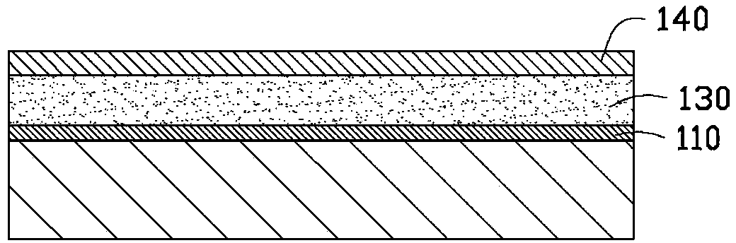
[0026] In the second step, see figure 2 , pressing the ...


PUM


Abstract

A circuit board with high-density circuits includes a dielectric layer, a plurality of metal pads embedded in the dielectric layer, a first conducting circuit layer and a second conducting circuit layer formed on two opposite surfaces of the dielectric layer, and a plurality of first through holes and a plurality of second through holes are formed in the dielectric layer. Each metal pad has a penetrating hole, each first through hole is communicated with a corresponding penetrating hole and a corresponding second through hole, the hole diameter of the penetrating hole is smaller than the hole diameters of the first through hole and the second through hole with which the penetrating hole is communicated, the communicated first through hole, second through hole and penetrating hole are filled with plated metal to form conducting holes, and the first conducting circuit layer and the second conducting circuit layer are electrically conducted through the conducting holes. The invention also provides a method for manufacturing the circuit board with the high-density circuits.

Description

technical field [0001] The invention relates to the technical field of circuit board production, in particular to a circuit board with high-density circuits and a production method thereof. Background technique [0002] Packaging substrates are used to carry chips and are widely used in various electronic products. In order to realize mutual conduction of circuits between different conductive circuit layers, via holes are usually made in the packaging substrate. For relatively high-end packaging substrates, it is necessary to use metal for plugging holes to obtain a packaging substrate with relatively stable performance. Since the packaging substrate is usually a hard board with a relatively thick dielectric layer, the through hole is usually formed by double-sided laser ablation, that is, the ablation is performed from the opposite sides of the dielectric layer, so that the holes formed by ablation on both sides The holes communicate with each other to obtain a through ho...

Claims


Application Information

Patent Timeline
Patent Type & Authority Applications(China)
IPC IPC(8): H05K1/11H05K3/42
Inventor 胡文宏
Owner QI DING TECHNOLOGY QINHUANGDAO CO LTD
Why Eureka
Try Eureka