

Method of processing shape of polytetrafluoroethylene (PTFE) printed circuit board
A polytetrafluoroethylene, shape processing technology, applied in the directions of printed circuit manufacturing, printed circuits, electrical components, etc., can solve the problems of high cost, difficult to obtain board surface quality, unfavorable production control, etc., to achieve the effect of saving production costs
Inactive Publication Date: 2014-10-15
SHANGHAI FAST PCB CIRCUIT TECH CORP LTD
View PDF3 Cites 4 Cited by
- Summary
- Abstract
- Description
- Claims
- Application Information
AI Technical Summary
Problems solved by technology
However, due to the good mechanical ductility of PTFE, the dynamic and static friction coefficient of steel is 0.04, which is smaller than that of nylon, polyoxymethylene and polyester plastics, so it is difficult to obtain a better surface for mechanical processing. Quality, poor machinability
[0004] The thickness of the printed board made of PTFE material is 0.5mm, and the size of the board is relatively small, only 3mm wide. Because the material of the board is relatively soft, using the normal milling method to operate the shape will cause the board to not be well stressed during the milling process, and the edge of the board will be damaged. Milling deformation; using laser milling, the energy will burn the board, and will melt the PTFE material, which cannot be effectively separated; it cannot be punched out with a knife mold, and can only be punched by a knife mold and an etching mold, but There is still deformation during the punching process, and the cost is relatively high, which is not conducive to production control
Method used
View moreImage
Smart ImageViewing Examples


Examples
Embodiment
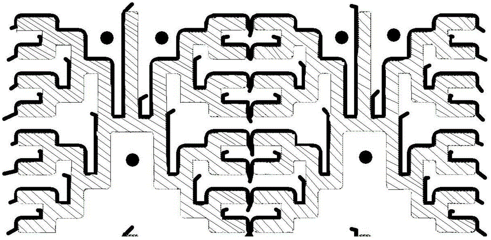
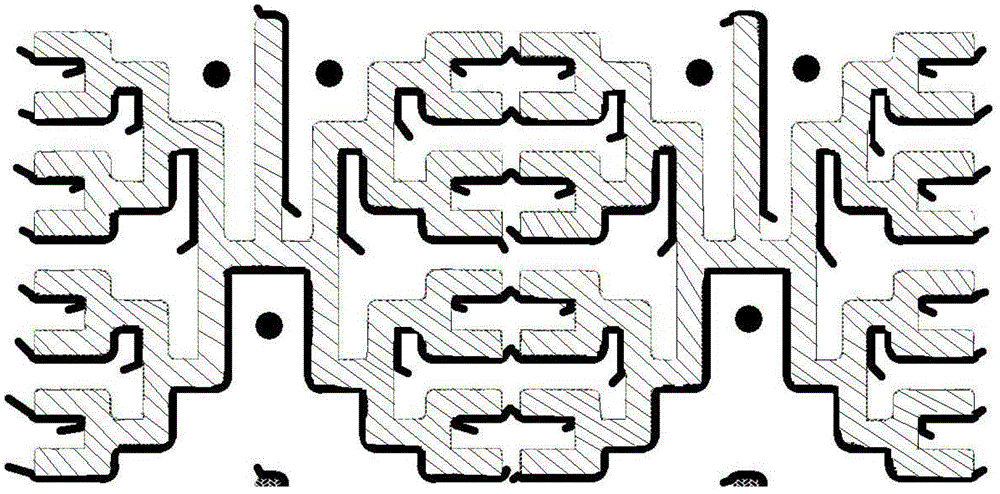
[0021] Such as figure 1 Shown is the profile of a polytetrafluoroethylene printed board with a thickness of 0.5 mm and a width of 3 mm. The present invention adopts two operations of milling the profile, first adding a 0.5 mm thick cover plate on the polytetrafluoroethylene printed board, and then using The first shape mold mills the shape of the printed board after being covered, and the first shape mold is half of the shape of the printed board, such as figure 2 shown; then replace a cover plate, and then use the second shape mold to mill the shape. The second shape mold is the other half of the printed board shape, such as image 3 shown.
Login to View More PUM
 Abstract
The invention relates to a method of processing the shape of a polytetrafluoroethylene (PTFE) printed circuit board. Two times of shape milling operation are adopted. The method comprises the following specific steps: a cover plate is additionally arranged on the PTFE printed circuit board, a first shape mold is used for carrying out shape milling on the printed circuit board additionally provided with the cover plate, replacement of a cover plate is carried out, and a second shape mold is used for carrying out shape milling. Compared with the prior art, a common machine can be directly adopted for carrying out shape milling, a knife mold mode and an etching mold mode do not need to be adopted for punching, and therefore a large amount of production cost is saved; and due to the operation of cover plate addition, any deformation and other quality problems do not happen to the plate during the shape milling process, and the method can be applied to mass production of the printed circuit boards.
Description
technical field [0001] The invention relates to a method for processing the shape of a printed board, in particular to a method for processing the shape of a polytetrafluoroethylene printed board. Background technique [0002] The shape processing of printed boards is an important link in the process of making printed boards, and it is also one of the difficulties. Printed board shape processing methods include milling shape, punching shape, opening "V" groove and drilling shape, among which the most commonly used method is milling shape. The milling profile processing method is mainly to process the PCB profile and internal profile on a CNC milling machine with a carbide tool. [0003] In the shape processing, ordinary epoxy glass cloth laminated board (FR-4) is relatively easy, but it is difficult for some special materials, polytetrafluoroethylene (PTFE) material is one of the important ones. PTFE material has excellent dielectric properties, and its electrical insulati...
Claims
Login to View More Application Information
Patent Timeline
 Patent Type & AuthorityApplications(China)
IPC IPC(8): H05K3/00
Inventor姚宇国
OwnerSHANGHAI FAST PCB CIRCUIT TECH CORP LTD