Selective nickel and gold plating method, PCB and device

A PCB board and electro-nickel-gold technology, which is applied in the field of selective electro-nickel-gold, can solve the problems such as the difficulty of electroplating nickel-gold on PCB boards, and achieve the effect of improving the bonding force

Active Publication Date: 2014-10-15
SHENNAN CIRCUITS
View PDF6 Cites 20 Cited by
  • Summary
  • Abstract
  • Description
  • Claims
  • Application Information

AI Technical Summary

Problems solved by technology

[0003] The invention provides a method for selective nickel-gold electroplating, which solves the problem of difficulty in electroplati

Method used


Image

  • Selective nickel and gold plating method, PCB and device
  • Selective nickel and gold plating method, PCB and device
  • Selective nickel and gold plating method, PCB and device

Examples


Embodiment Construction

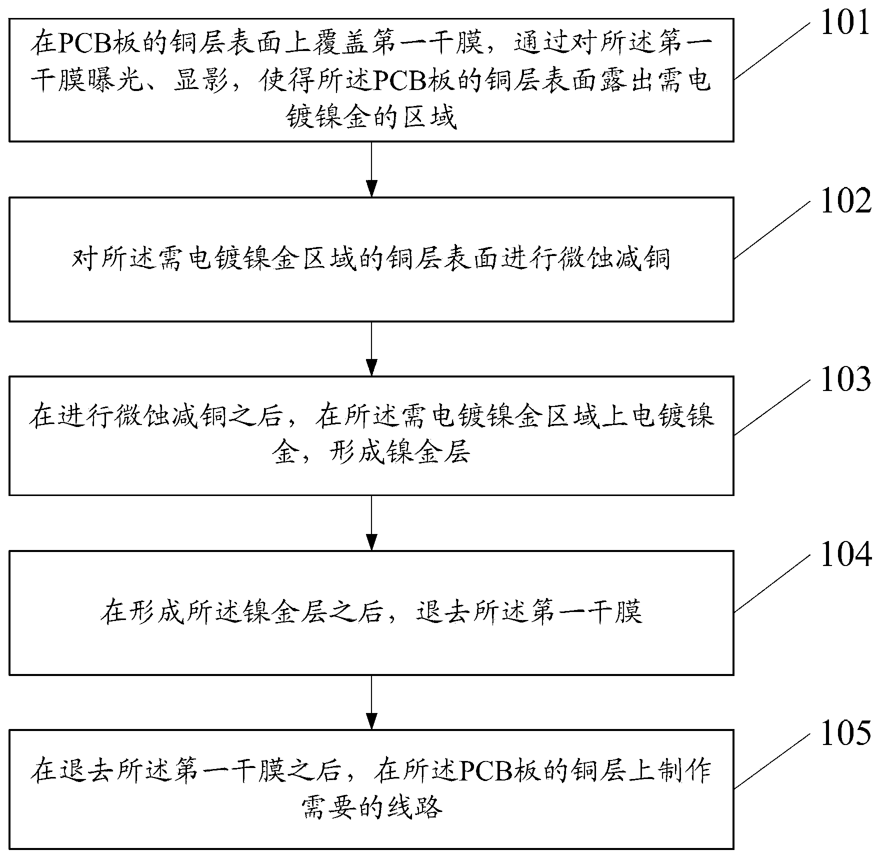
[0035] Such as figure 1 As shown, embodiment 1 of the present invention provides a kind of method of selective electric nickel gold, comprising:

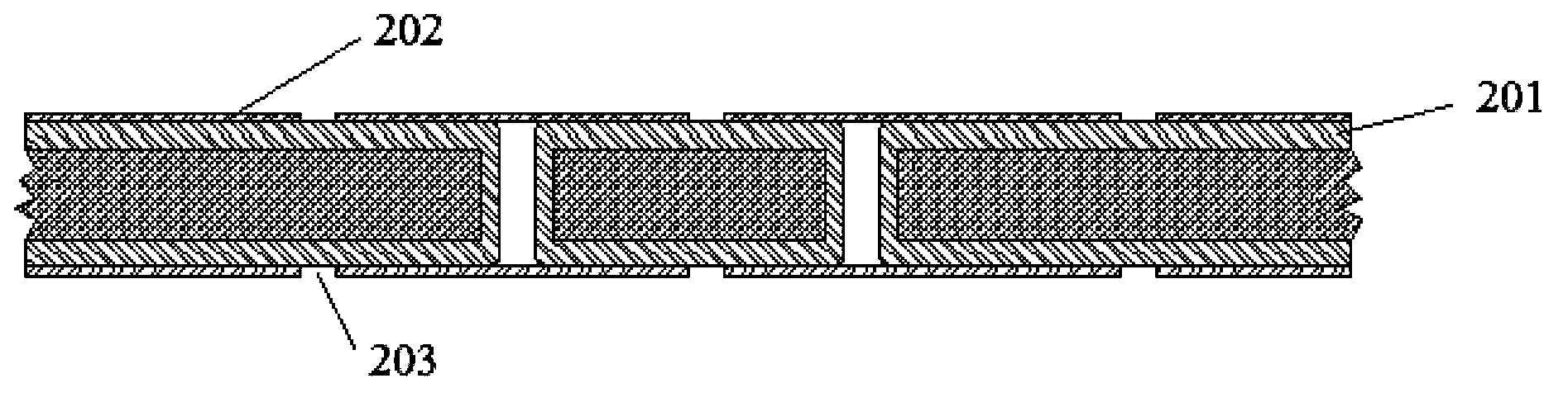
[0036] 101. If Figure 2a As shown, the first dry film 202 is covered on the surface of the copper layer 201 of the PCB board, and by exposing and developing the first dry film 202, the surface of the copper layer 201 of the PCB board exposes the area 203 that needs to be electroplated with nickel and gold. .

[0037] The area to be electroplated with nickel and gold may be a pad area for making inserts or mounting components. Electroplating nickel gold on the surface of the pad can improve the wear resistance and corrosion resistance of the pad surface.

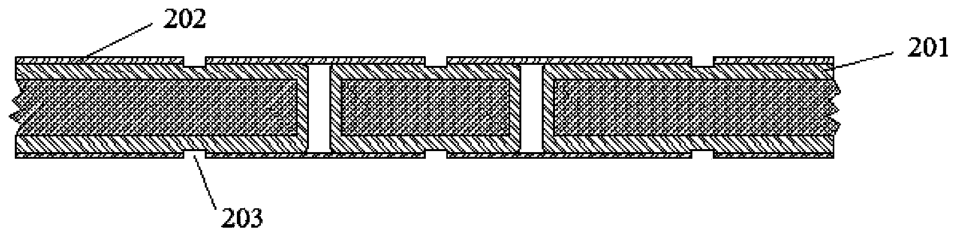
[0038] 102. Perform micro-etching to reduce copper on the surface of the copper layer in the region 203 to be electroplated with nickel and gold.

[0039] Such as Figure 2b As shown, the thickness of the surface of the copper layer in the region 203 to be electroplated with ...


PUM


Abstract

The invention discloses a selective nickel and gold plating method comprising the steps that a first dry film is covered on the surface of a copper layer of a PCB, and a area requiring nickel and gold plating is exposed out of the surface of the copper layer of the PBC via exposure and development; micro-etching and copper reduction are performed on the copper layer of the area requiring nickel and gold plating; and then nickel and gold are plated on the copper layer of the area requiring nickel and gold plating, then the first dry film is removed, and a required line is manufactured on the copper layer of the PCB. According to the method, nickel and gold are firstly plated on the surface of the copper layer of the PCB, and then the line is manufactured so that a lead wire for plating does not need to be manufactured in the overall implement process, and a problem of difficulty in nickel and gold plating on the PCB caused by the fact that the lead wire for plating cannot be manufactured on the PCB is solved. Besides, micro-etching and copper reduction are performed on the copper layer of the area requiring nickel and gold plating so that height difference between the nickel and gold surface of the nickel and gold area and the surface of the line without nickel and gold plating is reduced, and thus combination force of the dry film and the surface of the PCB in the subsequent dry film covering technology is enhanced.

Description

technical field [0001] The invention relates to the field of printed circuits, in particular to a selective electro-nickel-gold method, a printed circuit board (Printed Circuit Board, PCB) and a device. Background technique [0002] At present, in order to better tightly weld components and PCB boards, different materials are generally coated on different surface areas of the PCB board to form different coating layers. For example, electroplate nickel and gold on the surface of the socket hole and pad of the PCB, and coat the organic solderability preservatives (OSP) on the surface of the Ball Grid Array (BGA) of the PCB, so that the PCB The surface area covered with Ni-Au on the board has good wear resistance and corrosion resistance, and the surface area covered with OSP on the PCB has good solderability. In order to cover nickel-gold and OSP on different surface areas of the PCB board, the process of electroplating nickel-gold first and then making OSP is generally used ...

Claims


Application Information

Patent Timeline
IPC IPC(8): H05K3/06H05K3/24
Inventor 管育时陈于春武凤伍沙雷
Owner SHENNAN CIRCUITS
Why Eureka
Try Eureka