Low-power rapid-boost FLASH charge pump control circuit

A charge pump control, low power consumption technology, applied in the direction of control/regulation system, electrical components, adjusting electrical variables, etc. The effect of low consumption and increased speed

Active Publication Date: 2014-10-22
BEIJING MXTRONICS CORP +1
View PDF2 Cites 15 Cited by
  • Summary
  • Abstract
  • Description
  • Claims
  • Application Information

AI Technical Summary

Problems solved by technology

The traditional FLASH charge pump has the disadvantages of large power consumption and slow voltage boost when meeting normal working requirements, which is not conducive to the use of low-power products such as handheld devices and battery-powered products, as well as applications that require high programming and erasing speeds

Method used


Image

  • Low-power rapid-boost FLASH charge pump control circuit
  • Low-power rapid-boost FLASH charge pump control circuit
  • Low-power rapid-boost FLASH charge pump control circuit

Examples


Embodiment Construction

[0032] Below in conjunction with accompanying drawing and specific embodiment the present invention is described in further detail:

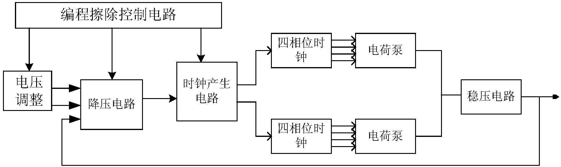
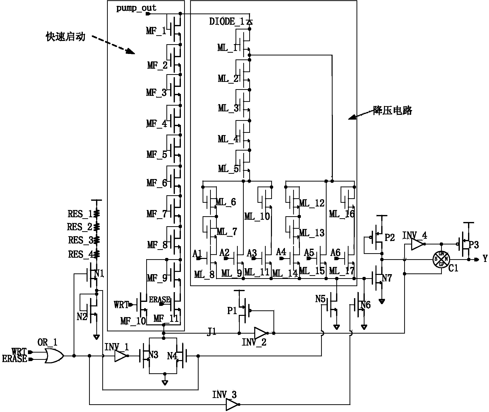
[0033] like figure 1 Shown is the structural block diagram of the low power consumption fast boost FLASH charge pump control circuit of the present invention, it can be seen from the figure that the low power consumption fast boost FLASH charge pump control circuit of the present invention is composed of a program erasure control circuit, a voltage adjustment circuit, a step-down circuit, Clock generation circuit, four-phase clock circuit, charge pump and voltage regulator circuit.

[0034] The programming and erasing control circuit controls the opening and closing of the voltage adjustment circuit, the step-down circuit and the clock generation circuit; when the FLASH is in the read operation, the step-down circuit, the voltage adjustment circuit and the clock generation circuit are turned off; when the FLASH is in the programming and erasing ...


PUM


Abstract

The invention relates to a low-power rapid-boost FLASH charge pump control circuit. The low-power rapid-boost FLASH charge pump control circuit comprises a programming erase control circuit, a voltage regulating circuit, a voltage reducing circuit, a clock generating circuit, a four phase clock circuit, a charge pump and a voltage stabilizing circuit. The voltage reducing circuit is divided into two paths, one path is used for quick start and works when the output voltage of the charge pump is low, the other path is used for the voltage trimming of the charge pump and works when the output voltage of the charge pump approaches a target value, and the voltage reducing circuit reduces the voltage through a reverser biased diode and a forward biased diode in order to reduce power consumption; the clock generating circuit is used for generating a clock required by the work of the charge pump, the frequency of the clock is adjustable, and in the early start stage, the clock runs in a fastest frequency within an adjustable range, and the voltage of the charge pump fast rises; and when the voltage of the charge pump approaches the target value, the clock frequency is trimmed according to the feedback voltage of the charge pump in order o maintain the voltage of the charge pump in a reasonable range. The control circuit reduces the power consumption of a Flash memory and increases the programming erasing speed of the Flash memory.

Description

technical field [0001] The invention belongs to the field of integrated circuits, and relates to a FLASH charge pump control circuit, in particular to a low-power fast boost FLASH charge pump control circuit, which is suitable for FLASH applications that require relatively strict power consumption and fast boosting of the charge pump. Background technique [0002] In embedded systems, Flash memory is a commonly used data and program storage device. With the continuous progress of semiconductor process technology, the Flash product line is becoming more and more abundant, and the market competition is particularly fierce. Flash design is also developing in the direction of high density, high speed, low power consumption, and low cost. The performance of Flash has become an important means for companies to compete in the market. [0003] Flash needs to be boosted during both programming and erasing operations, which requires higher requirements on the Flash charge pump. The ...

Claims


Application Information

Patent Timeline
Patent Type & Authority Applications(China)
IPC IPC(8): G11C16/06H02M3/156
Inventor 董哲
Owner BEIJING MXTRONICS CORP
Why Eureka
Try Eureka