

Organic light-emitting device and preparation method thereof
An electroluminescent device and luminescence technology, which is applied in the direction of electric solid-state devices, semiconductor/solid-state device manufacturing, electrical components, etc., can solve the problems of poor device stability, device luminous efficiency, low light extraction performance, and poor cathode electron injection ability, etc. question
- Summary
- Abstract
- Description
- Claims
- Application Information
AI Technical Summary
Problems solved by technology
Method used
Image

Examples
Embodiment 1
[0088] A method for preparing an organic electroluminescent device, comprising the following steps:
[0089] (1) Ultrasonic cleaning of the ITO glass substrate with detergent and deionized water for 15 minutes each to obtain a clean conductive anode glass substrate;
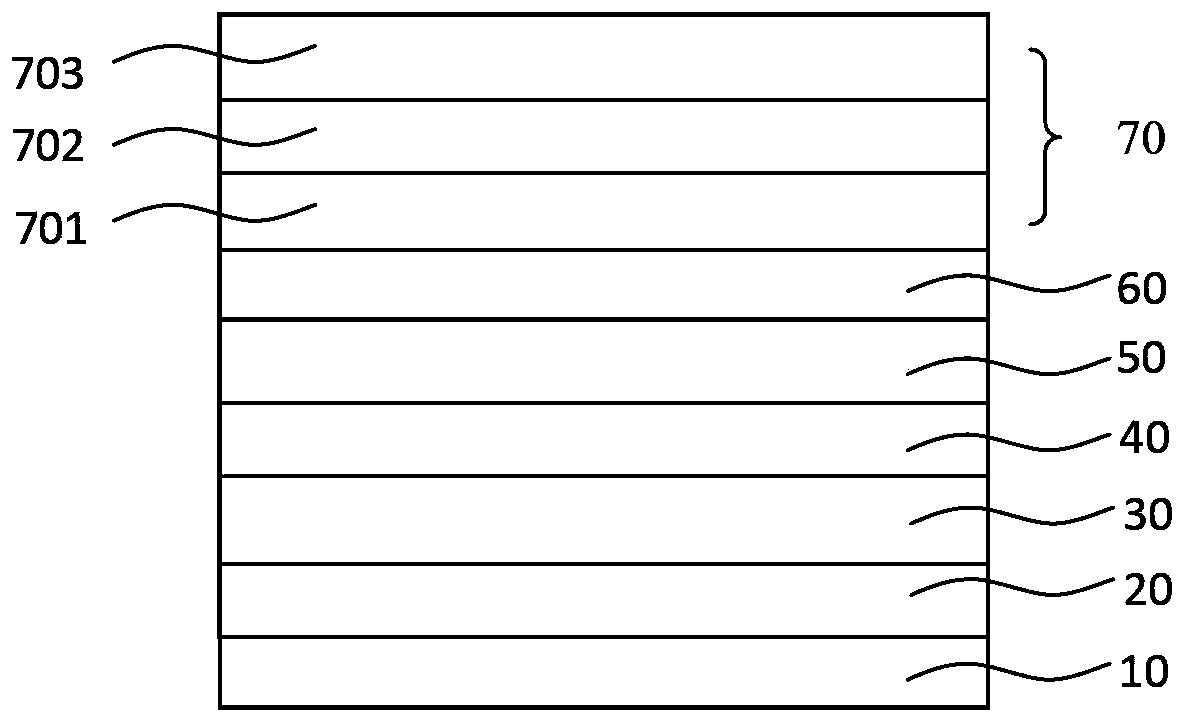
[0090] (2) In the high vacuum coating system (Shenyang Scientific Instrument Development Center Co., Ltd.), the pressure is 8×10 -5 Under the condition of Pa, on a clean conductive anode glass substrate, thermally resistively evaporated hole injection layer, hole transport layer, light emitting layer, electron transport layer and electron injection layer in sequence;
[0091] Specifically, in this embodiment, the material of the hole injection layer is MoO 3 , with a thickness of 40nm; the material of the hole transport layer is TCTA, with a thickness of 40nm; the material of the light-emitting layer is Alq3, with a thickness of 25nm; the material of the electron transport layer is TAZ, with a thickness of 120nm; ...
Embodiment 2
[0098] A method for preparing an organic electroluminescent device, comprising the following steps:
[0099] (1) Ultrasonic cleaning of the AZO glass substrate with detergent and deionized water for 15 minutes each to obtain a clean conductive anode glass substrate;
[0100] (2) In the high vacuum coating system (Shenyang Scientific Instrument Development Center Co., Ltd.), the pressure is 2×10 -3 Under the condition of Pa, on a clean conductive anode glass substrate, thermally resistively evaporated hole injection layer, hole transport layer, light emitting layer, electron transport layer and electron injection layer in sequence;
[0101] Specifically, in this embodiment, the material of the hole injection layer is WO 3 , with a thickness of 80nm; the material of the hole transport layer is TCTA, with a thickness of 60nm; the material of the light-emitting layer is ADN, with a thickness of 5nm; the material of the electron transport layer is Bphen, with a thickness of 200nm;...
Embodiment 3
[0107] A method for preparing an organic electroluminescent device, comprising the following steps:
[0108] (1) Ultrasonic cleaning of the IZO glass substrate with detergent and deionized water for 15 minutes each to obtain a clean conductive anode glass substrate;
[0109] (2) In the high vacuum coating system (Shenyang Scientific Instrument Development Center Co., Ltd.), the pressure is 5×10 -5 Under the condition of Pa, on a clean conductive anode glass substrate, thermally resistively evaporated hole injection layer, hole transport layer, light emitting layer, electron transport layer and electron injection layer in sequence;
[0110] Specifically, in this embodiment, the material of the hole injection layer is V 2 o 5 , with a thickness of 20nm; the material of the hole transport layer is TAPC, with a thickness of 30nm; the material of the light-emitting layer is BCzVBi, with a thickness of 40nm; the material of the electron transport layer is TAZ, with a thickness of ...
PUM
 Abstract
Description
Claims
Application Information