Organic electroluminescence device and manufacturing method of organic electroluminescence device

An electroluminescent device and luminescent technology, which is applied in the manufacture of organic semiconductor devices, electric solid devices, semiconductor/solid devices, etc., can solve the problems of low luminous efficiency of light emitting devices, unstable performance of light emitting devices, and easy reaction with water and oxygen, etc. problems, achieve excellent electron injection performance, avoid adverse effects, and achieve high luminous efficiency

Inactive Publication Date: 2014-04-16
OCEANS KING LIGHTING SCI&TECH CO LTD +2
View PDF0 Cites 2 Cited by
  • Summary
  • Abstract
  • Description
  • Claims
  • Application Information

AI Technical Summary

Problems solved by technology

In order to improve the carrier injection ability and reduce the starting voltage of the device, metal materials with low work function are usually used as the cathode, but the metal with low work function is too active and easily reacts with water and oxygen, making the performance of organic electroluminescent devices unstable. , low service life
Another method is to add an electron injection layer between the cathode and the organic layer. At present, the most commonly used halides of alkali metals such as lithium fluoride (LiF) and cesium fluoride (CsF) are used as the electron injection layer. Excellent performance and widely used, but the presence of halogen atoms in these materials will quench the luminescence, making the luminous efficiency of organic electroluminescent devices lower

Method used


Image

  • Organic electroluminescence device and manufacturing method of organic electroluminescence device
  • Organic electroluminescence device and manufacturing method of organic electroluminescence device
  • Organic electroluminescence device and manufacturing method of organic electroluminescence device

Examples


preparation example Construction

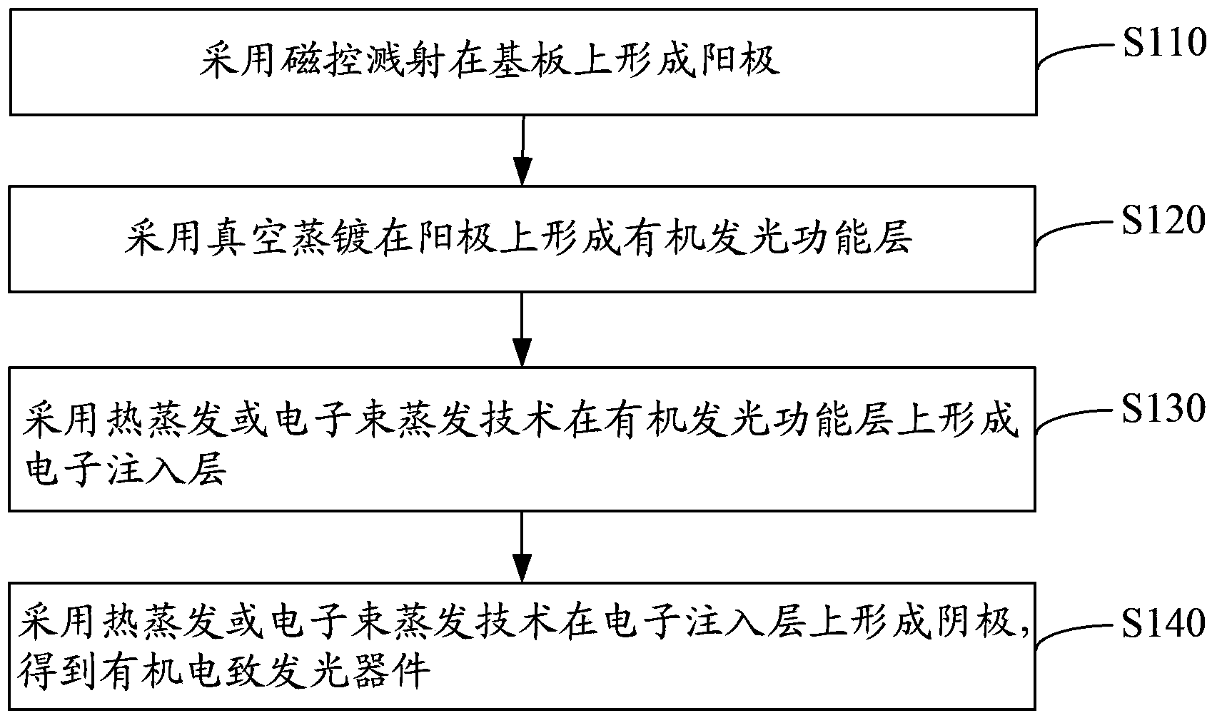
[0058] see figure 2 , the preparation method of the organic electroluminescent device of an embodiment, comprises the following steps:

[0059] Step S110: forming an anode on the substrate by magnetron sputtering.

[0060] The substrate adopts transparent glass or polyethersulfone resin substrate.

[0061] Firstly, the substrate is cleaned to prevent the pollutants on the substrate from adversely affecting the performance of the organic electroluminescent device. Place the substrate in deionized water containing detergent for ultrasonic cleaning. After cleaning, treat it with isopropanol and acetone in ultrasonic for 20 minutes, then dry it with nitrogen, and set it aside.

[0062]A metal thin film is formed on a dry and clean substrate by magnetron sputtering to obtain an anode. The material of the anode is indium tin oxide (ITO), indium zinc oxide (IZO), aluminum zinc oxide (AZO) or gallium zinc oxide (GZO). The thickness of the anode is 100 nm.

[0063] Step S120: For...

Embodiment 1

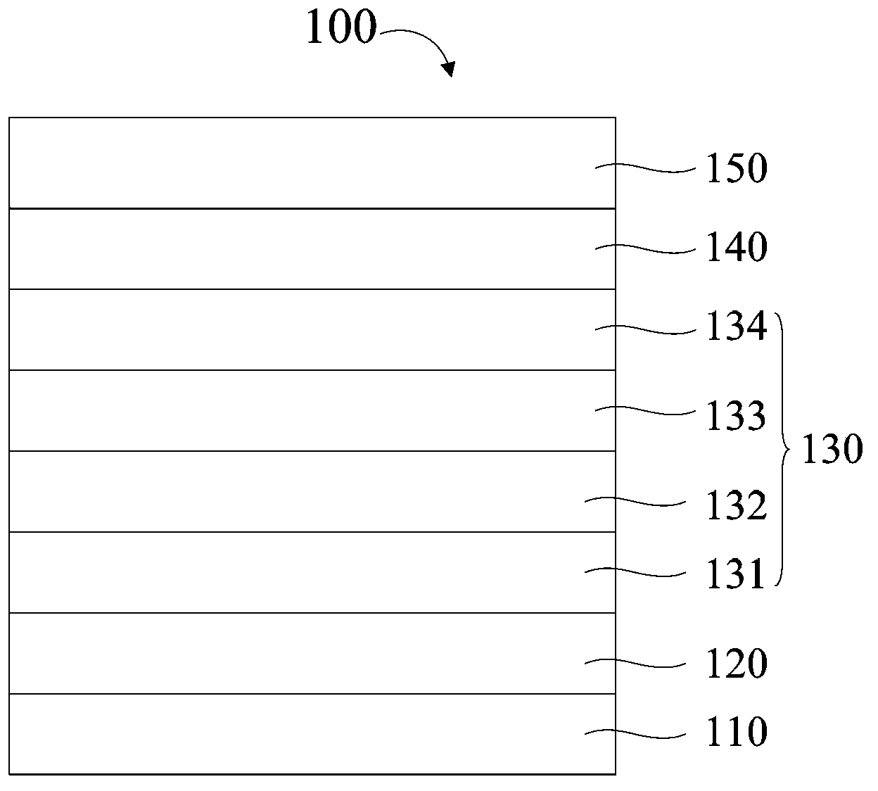
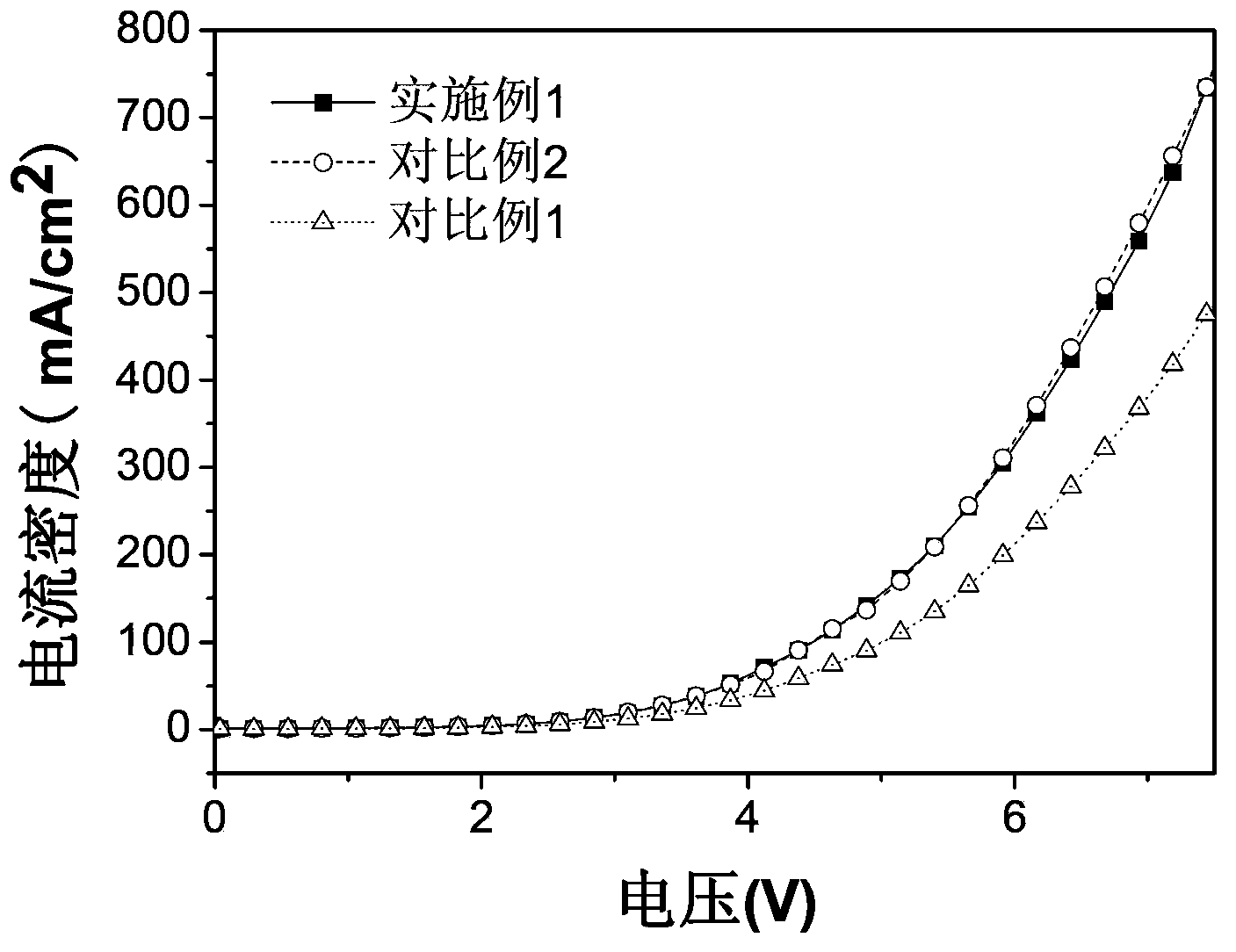
[0092] The structure is: Glass / ITO / CuPc / NPB / Ir(MDQ) 2 (acac):NPB / TPBi / Ba(OH) 2 : Al / Al Organic Electroluminescent Devices

[0093] The preparation method of the organic electroluminescent device is as follows:

[0094] (1) Provide transparent glass as the substrate, denoted as Glass. Put the transparent glass in deionized water containing detergent for ultrasonic cleaning. After cleaning, use isopropanol and acetone in ultrasonic treatment for 20 minutes, and then blow dry with nitrogen;

[0095](2) An anode is formed on the substrate by thermal evaporation. The material of the anode is indium tin oxide (ITO), and the thickness of the anode is 100 nanometers. After preparing the anode, put the anode laminated on the surface of the transparent glass into the plasma treatment chamber for 10 minutes;

[0096] (3) A hole injection layer is formed on the anode by vacuum evaporation. Vacuum degree is 5×10 -4 Pa. The material of the hole injection layer is copper phthalocyani...

Embodiment 2

[0103] The structure is: Glass / ITO / ZnPc / α-NPD / DCJTB:Alq 3 / PBD / Ba(NO 3 ) 2 / Yb organic electroluminescent devices

[0104] The preparation method of the organic electroluminescent device is as follows:

[0105] (1) Provide transparent glass as the substrate, denoted as Glass. Put the transparent glass in deionized water containing detergent for ultrasonic cleaning. After cleaning, use isopropanol and acetone in ultrasonic treatment for 20 minutes, and then blow dry with nitrogen;

[0106] (2) An anode is formed on the substrate by thermal evaporation. The material of the anode is indium tin oxide (ITO), and the thickness of the anode is 100 nanometers. After preparing the anode, put the anode laminated on the surface of the transparent glass into the plasma treatment chamber for 10 minutes;

[0107] (3) A hole injection layer is formed on the anode by vacuum evaporation. Vacuum degree is 5×10 -4 Pa. The material of the hole injection layer is zinc phthalocyanine (ZnPc...


PUM

PropertyMeasurementUnit
Thicknessaaaaaaaaaa
Thicknessaaaaaaaaaa
Thicknessaaaaaaaaaa

Abstract

The invention relates to an organic electroluminescence device which comprises a substrate, a positive pole, an organic luminescent functional layer, an electronic injection layer and a negative pole, wherein the substrate, the positive pole, the organic luminescent functional layer, the electronic injection layer and the negative pole are sequentially arranged in an overlaid mode. The electronic injection layer is made of a mixture composed of barium compounds and metal. The barium compounds are selected from one of barium hydroxide, barium carbonate, barium nitrate and barium sulfate, and the metal is selected from one of silver, aluminum, samarium, ytterbium and alloy of the silver, the aluminum, the samarium and the ytterbium. In the mixture, the mass percent of the barium compounds is 35-80%. The mixture composed of the barium compounds and the metal has the excellent electronic injection performance, the electronic mobility can be improved, the starting voltage of the organic electroluminescence device can be reduced, the quenching harmful effect of halogen atoms on emitted light can be avoided, and the luminous efficiency is high. The invention further provides a manufacturing method of the organic electroluminescence device, another organic electroluminescence device and the manufacturing method of the organic electroluminescence device.

Description

technical field [0001] The invention relates to the technical field of light emission, in particular to two organic electroluminescent devices and a preparation method thereof. Background technique [0002] Organic Light Emission Diode, hereinafter referred to as OLED, has the characteristics of high brightness, wide range of material selection, low start-up voltage, full-cured active light, etc., and has the advantages of high definition, wide viewing angle, and fast response speed. It is a display technology and light source with great potential, which conforms to the development trend of mobile communication and information display in the information age, as well as the requirements of green lighting technology, and is the focus of many researchers at home and abroad. [0003] So far, although researchers from all over the world have greatly improved the performance indicators of organic electroluminescent devices by selecting suitable organic materials and rational devic...

Claims


Application Information

Patent Timeline
IPC IPC(8): H01L51/50H01L51/54H01L51/56
CPCH10K50/171H10K2102/00H10K71/00
Inventor 周明杰王平冯小明张振华
Owner OCEANS KING LIGHTING SCI&TECH CO LTD
Why Eureka
Try Eureka