Wafer silicon through hole structure and preparation method thereof
A technology of through-silicon vias and wafers, applied in the field of microelectronics, can solve the problems of limited space for increasing the thickness of silicon dioxide insulating layer, expensive high-resistance silicon, slow oxidation speed, etc., so as to weaken the electric field density and reduce the effective contact , the effect of reducing the thermal stress effect
Active Publication Date: 2014-11-12
NAT CENT FOR ADVANCED PACKAGING
View PDF3 Cites 6 Cited by
- Summary
- Abstract
- Description
- Claims
- Application Information
AI Technical Summary
Problems solved by technology
High-resistance silicon is more expensive, and it is only suitable for 2.5D silicon adapter boards, not for 3D active chip through-silicon vias
The space for increasing the thickness of the silicon dioxide insulating layer is limited. For thermally oxidized silicon dioxide, the oxidation rate is very slow after the thickness is greater than 1 micron. The increase in the thickness of silicon dioxide grown by PECVD will cause stress and cracking problems.
Method used
View moreImage
Smart ImageViewing Examples

Examples
Embodiment 1
Embodiment 2
Embodiment 3
Login to View More PUM
 Abstract
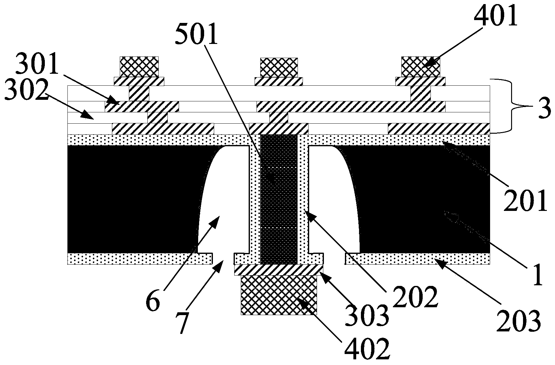
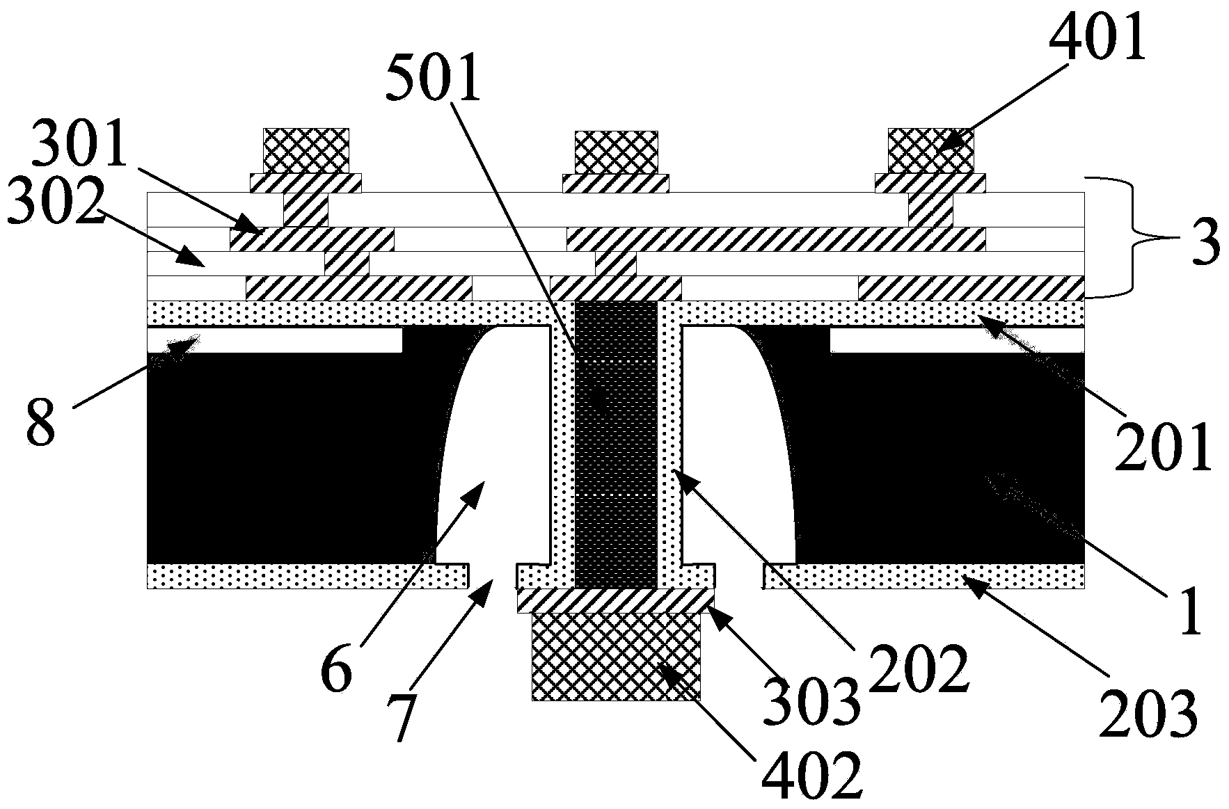
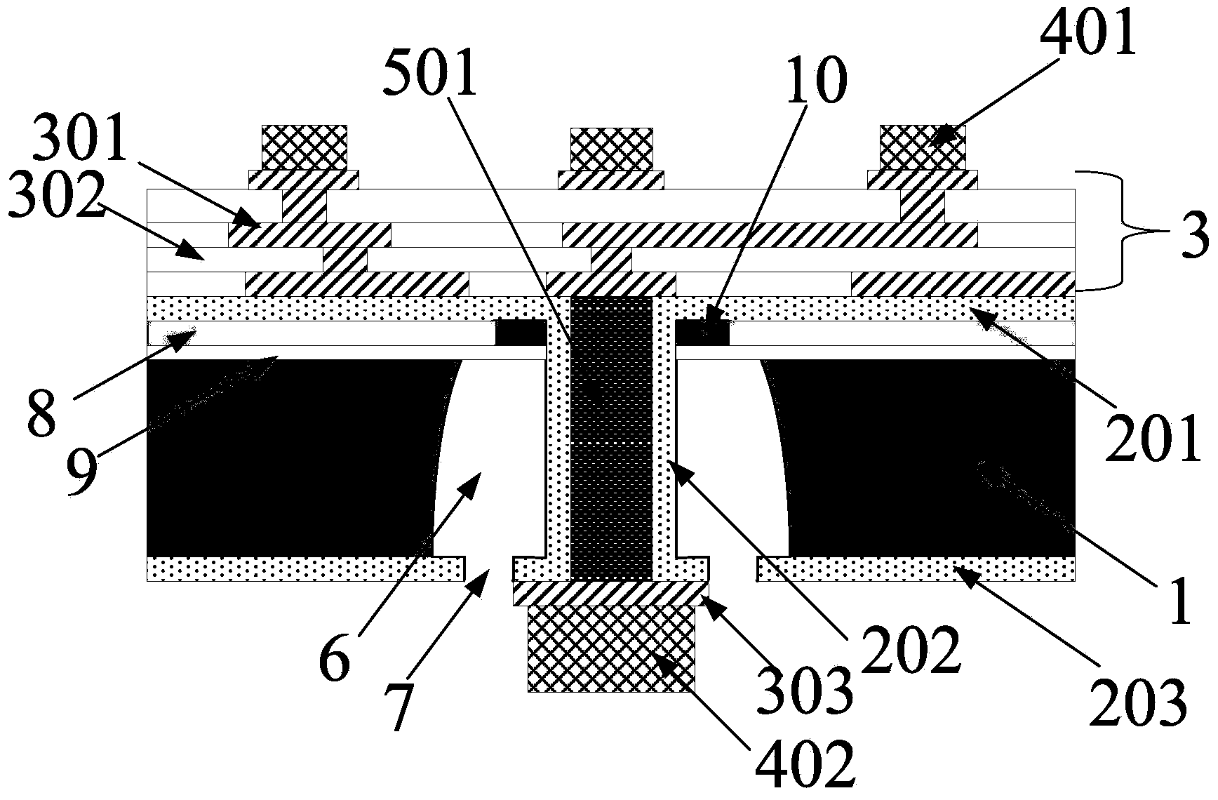
The invention belongs to the field of micro electronic techniques and discloses a wafer silicon through hole structure. The wafer silicon through hole structure comprises a through hole, a front passivation layer, a through hole passivation layer, a back passivation layer and a cavity in the periphery of the through hole passivation layer. The through hole is formed in a silicon substrate of a wafer, the through hole passivation layer is arranged on the lateral wall in the through hole, the front passivation layer and the back passivation layer are arranged on the front face and the back face of the silicon substrate and are respectively connected with the through hole passivation layer, and the cavity is formed in the periphery of the through hole passivation layer and in the silicon substrate. The thermal stress effect caused by large difference between coefficients of thermal expansion of through hole metal and silicon materials is reduced by forming the cavity outside the through hole in the wafer silicon substrate. Meanwhile, electric field density of the periphery of the through hole is greatly reduced so as to reduce high frequency loss of the through hole.
Description
technical field The invention relates to the technical field of microelectronics, in particular to a wafer through-silicon hole structure. Background technique With the consumer market's increasing demand for electronic products with small size, multi-function, low power consumption, and high performance, planar integrated circuits are facing huge challenges, and the feature size of CMOS is gradually approaching the physical limit. "Ultramole", 2.5-dimensional and 3-dimensional integration technology based on through-silicon via (Throuth-silicon-Via TSV) is expected to become a new driving force for the development of electronic integration technology. The structural design, fabrication process, physical parameter extraction and modeling of TSVs have become research hotspots. Since silicon is a semiconductor material with a forbidden band width of only 1.12eV, even intrinsic silicon has a certain degree of conductivity at room temperature, and in actual use, it usually pre...
Claims
Login to View More Application Information
Patent Timeline
 Patent Type & Authority Applications(China)
IPC IPC(8): H01L23/528H01L21/768
Inventor 李宝霞
Owner NAT CENT FOR ADVANCED PACKAGING