[0050] The present invention will be further described below in conjunction with the drawings and specific embodiments.
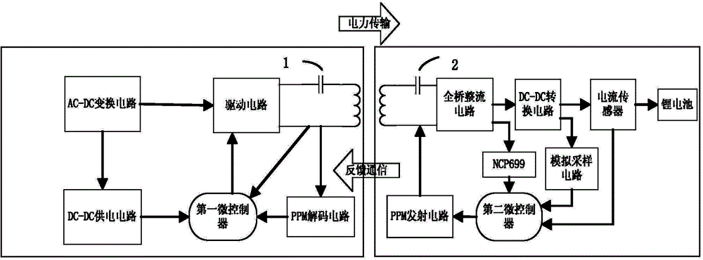
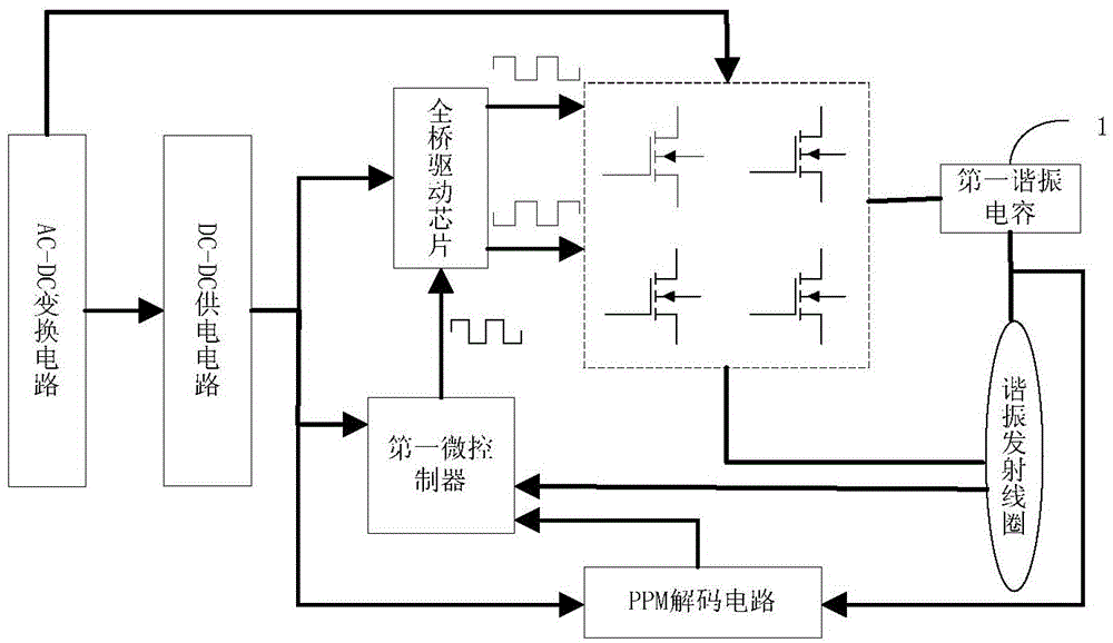
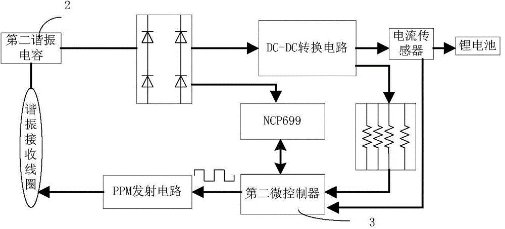
[0051] Such as figure 1 As shown, a wireless charging device is characterized by comprising a wireless charging transmitter and a wireless charging receiver. The wireless charging transmitter drive circuit excites the primary coil at a specific frequency. The resonant primary coil and the first resonant capacitor 1 connected in series generate LC resonance to generate electromagnetic waves. The wireless charging receiver receives electromagnetic energy through an LC matching circuit and passes DC-DC The conversion circuit charges the lithium battery.
[0052] Further, the microcontroller of the wireless charging receiver samples the output voltage and current through an analog sampling circuit and a current sensor, and combines and encodes the analog signals, and the generated PPM signal communicates the charging information to the primary coil through the secondary coil.
[0053] Such as figure 2 As shown, the wireless charging transmitter includes an AC-DC conversion circuit, a DC-DC power supply circuit, a driving circuit, a first microcontroller, a PPM decoding circuit, and a resonance transmitting circuit.
[0054] The main function of the first microcontroller is: sampling the peak value of the AC voltage on the primary coil, fine-tuning the PWM output pulse frequency, and stabilizing the resonant transmission power; performing pulse position modulation digital decoding on the signal processed by the PPM decoding circuit; through PCA The module outputs 120kHZ PWM drive pulse output to the drive chip; by detecting the peak-to-peak value of the sampled output voltage, it can be judged whether there is metal foreign matter on the transmitter base. If the sampled peak voltage is within ±5% of the resonance peak voltage, the PWM will be turned off Pulse signal to stop charging.
[0055] In the LC resonance system, there is a certain error in the matching of the resonance capacitance and inductance. When the LC resonance, the actual resonance capacitance and inductance error will match the original design resonance point combination, resulting in inconsistent LC resonance points during mass production, and the transmission power is consistent with the design The predetermined value is deviated (exceeding ±2%), which reduces the product qualification rate. The LC resonance system has several important characteristics: first, the combined resonance curve of each group of resonant coils and capacitors is different; second, the curve is different under different driving voltages; third, detecting whether there are metal foreign objects when the transmitter is working . In this way, the actual resonant frequencies of the required resonant coils and capacitors, as well as their typical curves and their parameters without metal foreign objects, have been determined by summing up a large amount of experimental data before the wireless charger leaves the factory. The typical curve of the coil is burned by scanning. Write to the EEPROM of the circuit. After leaving the factory, each group of wireless charging systems has its own typical curve record. When working, the first microcontroller compares the difference between the amplitude state at the center operating frequency and the typical value by looking up the table. If the amplitude voltage is lower than the typical value of the amplitude voltage at this time, the first microcontroller increases the center operating frequency by looking up the table to increase the amplitude; the amplitude voltage is higher than the typical value of the amplitude voltage, the first microcontroller reduces the center operation Frequency reduces the amplitude. At this time, the specific increase and decrease of the center working frequency are based on the control law in the table (summarized by a large number of experiments), and each frequency corresponds to an amplitude value. The resonant frequency set in this system is 150kHZ, the center working frequency is 120kHZ, the frequency resolution is 1kHZ, the lower limit of the resolution frequency is 90kHZ-120kHZ, and the upper limit is 120kHZ-150kHZ. The above control method is frequency nonlinear correction. Through frequency non-linear correction technology, the achieved effect is: realize frequency conversion, adjust power, stabilize transmission and charging power; eliminate LC error, keep the transmission power error at ±2% during mass production; detect whether there are metal foreign objects with safety hazards .
[0056] When the transmitter module is powered on, the initial center operating frequency is 120kHZ. The first microcontroller analyzes the sampled peak-to-peak voltage, compares it with the typical value, and uses frequency non-linear correction technology to make the frequency range from 90kHZ to 150kHZ with a resolution of 1KHZ and 120KHZ as the center to stabilize the transmission power.
[0057] In a resonant system, when the PWM output pulse frequency is equal to the resonant frequency, the resonance amplitude is the largest. The larger the amplitude, the larger the output power. Set the PWM output pulse frequency to be lower than the resonance frequency. When the PWM output frequency is far from the resonance frequency, the amplitude decreases; when the PWM output frequency is close to the resonance frequency, the amplitude increases. According to this principle, the output power can be adjusted by adjusting the PWM output pulse frequency.
[0058] The AC-DC conversion circuit is composed of an AC-DC power supply module and its peripheral circuits. It mainly performs the following functions: output 15V DC voltage as the main voltage of the wireless charging transmitter, acting on the upper arm of the full bridge circuit, and the output power is 15W, which is DC -DC power supply circuit power supply. The AC-DC power supply module selects AKF-15S15 from MinMAX Company.
[0059] The DC-DC power supply circuit is mainly composed of a 5V power supply module and a 3.3V power supply module. The 5V power supply module is used as the boost voltage of the PWM output signal of the first microcontroller, and is used as the input voltage of the 3.3V power supply module; 3.3V module Power the first microcontroller. The 5V power supply module chooses TI’s TPS54231D switching regulator chip, and the 3.3V power supply module chooses the AMS1117-3.3 chip.
[0060] The drive circuit is mainly composed of a full-bridge drive chip and a full-bridge topology circuit, which mainly completes the following functions: the full-bridge chip receives the PWM drive pulse of the first microcontroller, converts its level and amplifies the power, and outputs two channels of certain frequency, The PWM drive pulses with a phase difference of 180 degrees respectively drive the upper and lower diagonal power MOS transistors of the full bridge circuit. The output frequency of the full-bridge topology circuit is 120kHz, and the peak-to-peak value is 30V AC positive and negative square wave. Among them, the full-bridge driver chip selects Philips' high-power driver chip UBA2032T.
[0061] The resonant transmitting circuit is composed of the first resonant capacitor 1 and the resonant primary coil through series resonance, and mainly completes the following functions: the first resonant capacitor 1 and the primary coil generate resonant electromagnetic waves under the excitation of AC positive and negative square waves; the primary coil Also used as a communication coil. The central working frequency of the invention is set to 120kHZ, the capacitor and the coil are in accordance with For parameter matching, the resonance frequency is 150KHZ. As a key component, the capacitor is a high-power multi-level resonant capacitor, and the coil is a high-quality inductive coil.
[0062] The PPM decoding circuit is mainly composed of a buffer circuit, a signal amplifier circuit, a second-order band pass filter circuit, and a hysteresis comparison circuit. Its working principle: When the charging system is working, the PPM decoding circuit receives the PPM modulation information sent by the wireless receiver received on the primary coil and is first buffered and output by the emitter follower composed of the operational amplifier, and then the signal amplifying circuit and the second-order band pass The filter circuit performs amplification and filtering, sends it to the hysteresis comparator for pulse shaping, and converts the 50kHZ PPM modulation signal into a pulse signal that can be read by the first microcontroller. The circuit consists of a four-way operational amplifier LM324 and its peripheral components.
[0063] Such as image 3 As shown, the wireless receiver is mainly composed of LC resonance circuit, full bridge rectifier circuit, DC-DC conversion circuit,
[0064] It is composed of analog sampling circuit, second microcontroller and PPM transmitting circuit.
[0065] In the receiver LC resonant circuit, the second resonant capacitor 2 and the secondary coil are connected in series, and the capacitor and the coil are in accordance with For parameter matching, the parameter matching comprehensively considers the receiving efficiency. As a key component, the capacitor uses high-power multi-level resonant capacitors, and the coil uses high-quality inductance coils.
[0066] The full bridge rectifier circuit is formed by overlapping four Schottky rectifier tubes SS39 to rectify the induced voltage.
[0067] The DC-DC conversion circuit is composed of a switching regulator chip and its peripheral circuits. Its main functions are as follows: chopping and stepping down the 10V DC voltage output by the full-bridge rectifier circuit to 5 V, and charging the lithium battery. Taking into account that the charging power of the flat lithium battery is 10W, the DC-DC switching regulator chip adopts the LM2596-5 produced by NS Company, so that the maximum output power of the receiver is 15W under normal charging conditions.
[0068] Such as image 3 As shown, the second microcontroller samples the charging current output by the DC-DC converter, and performs four-channel analog sampling on the output 5V voltage. The four-channel sampling points are the output charging voltage after voltage division to improve the sampling Accuracy is good for coding. The sampled voltage and current signals are input to the microcontroller after RC low-pass filtering. The second microcontroller performs digital pulse modulation coding (PPM) on the four analog voltage and current signals, and sends out the corresponding pulse sequence to drive the PPM transmitter circuit . The specific principle is: the second microcontroller first outputs a frame synchronization pulse of a certain width, and then the second microcontroller samples the current signal and the four-channel output analog voltage signal, in which the four-channel analog sampling value is averaged to improve the sampling Accuracy, and A/D conversion is performed on the calculated average voltage and current value. Then the counter is decremented by 1, and when the counter is reduced to 0, the second microcontroller outputs PPM sequence pulses. Demodulation is based on the relative position of each pulse, and the digital signal can be obtained by judging the time interval between the PPM pulse and the synchronization pulse during demodulation. The second microcontroller samples the output voltage through the analog sampling circuit. When the voltage of the lithium battery is full, the second microcontroller sends a shutdown signal to the NCP699 to stop the charging action to protect the battery.
[0069] The PPM transmitting circuit is composed of an optocoupler and a switch MOS tube: the high-speed optocoupler receives the pulse sequence sent by the second microcontroller, and the pulse sequence is amplified by level power to drive the switching MOS tube, and the open-drain output of the switch tube will pass the feedback data packet through The secondary coil is sent to the wireless charging transmitter. The first microcontroller reads the charging feedback information, thereby knowing the charging power demand of the charging terminal. The first microcontroller uses a built-in algorithm program to increase the PWM output pulse frequency to move toward the resonance frequency when the charging power is lower than the preset charging power, and the resonance amplitude increases to increase the charging power; when the charging power is higher than When the charging power is preset, the PWM output pulse frequency is reduced to keep it away from the resonance frequency, and the resonance amplitude is reduced to reduce the charging power. In this way, the charging power is maintained constant.
[0070] The present invention selects PPM (Pulse Position Modulation) modulation mode, the feedback data packet is defined as Figure 4 As shown, including: packet header identification, used to specify the data packet transmission data content; ID identification, used to identify the data packet; data code group, used to transmit output current and voltage data information; data checksum, used to transmit Error codes in the process are checked to reduce the error rate. Table 1 below shows the structure of the feedback data packet.
[0071] Table 1 Feedback data packet structure
[0072]
[0073] Further, if the wireless charging transmitter does not receive the data packet sent by the wireless charging receiver after power-on, the wireless charging transmitter does not emit electromagnetic energy and is in a standby state until the feedback data packet is received. The wireless charging transmitter is identified by the ID flag bit of the received data packet. The charging process of the wireless charging power supply is: when the transmitter board is powered on, the transmitter board transmits power to the receiver board. At this time, the transmitter board does not receive the feedback signal of the receiver board (PPM transmission protocol) and is in a standby state; the secondary coil receives electromagnetic energy, The voltage is induced to supply power to the receiving system, the microcontroller starts to work and generates a feedback signal, which is fed back to the transmitter board through power amplification, and the transmitter board changes from the standby state to the working state after receiving the feedback signal.